Clock signal generating circuit, display panel module, imaging device, and electronic equipment

a clock signal and generating circuit technology, applied in the field of delay synchronization loop type signal generating circuit, can solve the problems of difficult inclusion on the panel, reduced circuit scale, and negligible delay difference between video signal and clock signal occurring at the display substrate, so as to reduce the number of delay stages and increase the resistance

Active Publication Date: 2011-02-01
JAPAN DISPLAY WEST
View PDF19 Cites 4 Cited by
  • Summary
  • Abstract
  • Description
  • Claims
  • Application Information

AI Technical Summary

Benefits of technology

[0008]A method has been conceived to reduce the delay difference between clock signals and video signals by using a phase regulator circuit such as a PLL (phase-locked loop) or DLL (delay-locked loop) circuit so as to approximate zero for the delay difference.
[0012]That is to say, the delay line is preferably of a two-stage configuration for coarse adjustment and fine adjustment, with ring-type shift registers and delay control units being provided to each stage. In this case, phase synchronization can be performed in a shorter time as compared with delay amount adjustment operations with a single delay line.
[0013]Further, the shift clock which drives the first and second ring-type shift registers may have a frequency lower than the first clock signal or the second clock signal. For example, the shift clock signal may be provided as frequency division output of the first clock signal. Using a shift lock with a low frequency in this way allows the operating margin of the shift register to improve. Accordingly, yield can be improved and manufacturing costs reduced.
[0014]The frequency of the first shift lock signal input to the first ring-type shift register may be lower than the frequency of the second shift lock signal input to the second ring-type shift register. That is to say, setting frequency of the first shift lock signal input to the first ring-type shift register so as to be lower than the frequency of the second shift lock signal input to the second ring-type shift register ultimately enables the operating margin of the coarse shift register to be higher than the operating margin of the fine shift register.
[0018]In this case as well, the shift clock which drives the ring-type shift register may have a frequency lower than the first clock signal or the second clock signal. Using a shift lock with a low frequency in this way allows the operating margin of the shift register to improve.
[0025]Applying the clock signal generating circuit of the configuration described above enables small circuit scale to be realized in a case of forming the circuit with thin-film transistors with high on resistance. Particularly, the greater the number of delay stages is, the more the circuit scale can be reduced in comparison with that of the related art.

Problems solved by technology

However, with recent system displays where the input frequency of video signals is very high, difference in delay between the video signal and the clock signal occurring at the display substrate is no longer negligible.
However, there is a problem with forming or printing active elements making up the clock signal generating circuit on the insulating substrate as thin-film transistors, in that inclusion on the panel is difficult due to the circuit scale thereof.
Particularly, a problem can be easily foreseen where the circuit scale becomes great in the event of configuring portions regarding which delay amount is to be set in the form of digital circuits.
Increased circuit scale leads to poor theoretical yield, which in turn leads to increased costs.

Method used


Image

  • Clock signal generating circuit, display panel module, imaging device, and electronic equipment
  • Clock signal generating circuit, display panel module, imaging device, and electronic equipment
  • Clock signal generating circuit, display panel module, imaging device, and electronic equipment

Examples


first embodiment

A First Embodiment

[0066]The following is a description regarding a case wherein the display panel is a liquid crystal display panel.

A-1 Configuration of Display Panel

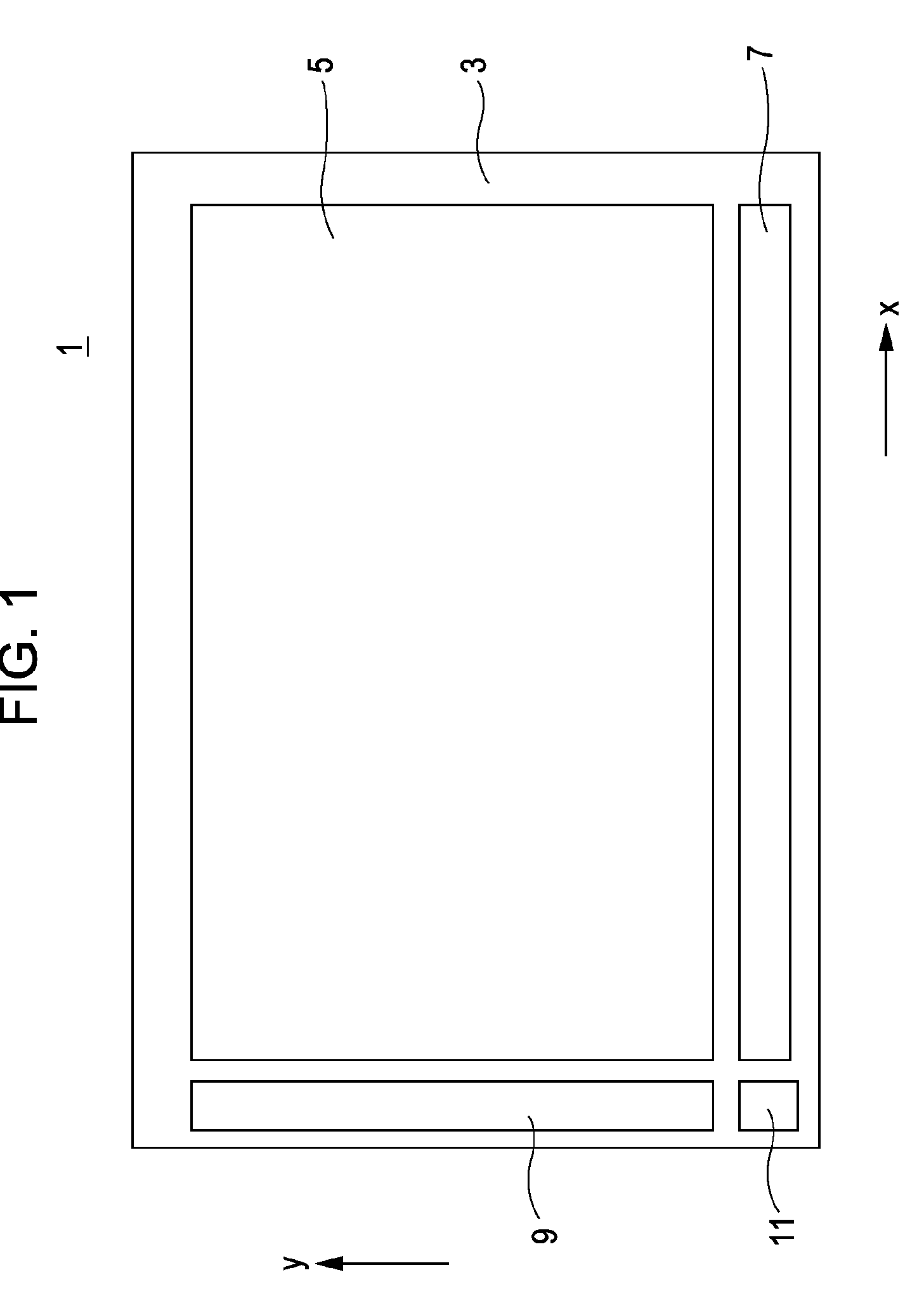
[0067]FIG. 1 illustrates a plan view configuration of a display panel 1 to be described in the present embodiment. In the case of this embodiment, a display region 5 and the peripheral circuits thereof are formed together with the same process on the face of the glass substrate 3. That is to say, we will assume a case wherein the display panel 1 is a system panel.

[0068]Gate lines and signal lines are formed in lattice form on the display region 5 in accordance with the resolution, and pixel circuits are formed at each intersection position thereof. That is to say, the display region 5 has a panel configuration corresponding to the active matrix driving method. Note that gate lines are wiring extending in the x direction of the display region, and signal lines are wiring extending in the y direction of the display region...

second embodiment

B Second Embodiment

B-1 Configuration of Display Panel

[0112]FIG. 13 illustrates a plan view configuration of a display panel 91 to be described in the present embodiment. In FIG. 13, components corresponding to FIG. 1 are denoted with the same reference numerals. As shown in FIG. 13, the display panel 91 differs from the display panel 1 shown in FIG. 1 only regarding the configuration of the clock signal generating circuit 93.

B-2 Configuration of Clock Signal Generating Circuit

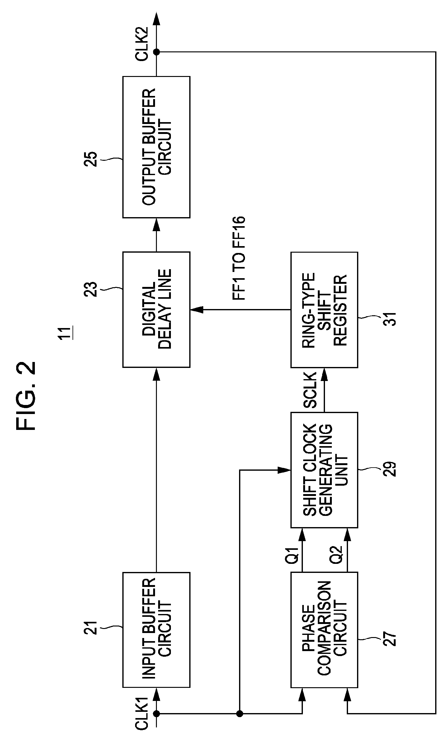
[0113]FIG. 14 illustrates an internal configuration example of a delay synchronization loop type clock signal generating circuit 93, proposed by the present Inventors in the present Specification. Components in FIG. 14 which are the same as those in FIG. 2 are denoted with the same reference numerals.

[0114]The clock signal generating circuit 93 in FIG. 14 includes an input buffer circuit 21, a voltage control type delay line 23, a digital delay line 101, an output buffer circuit 25, a phase comparison circuit 2...

third embodiment

C Third Embodiment

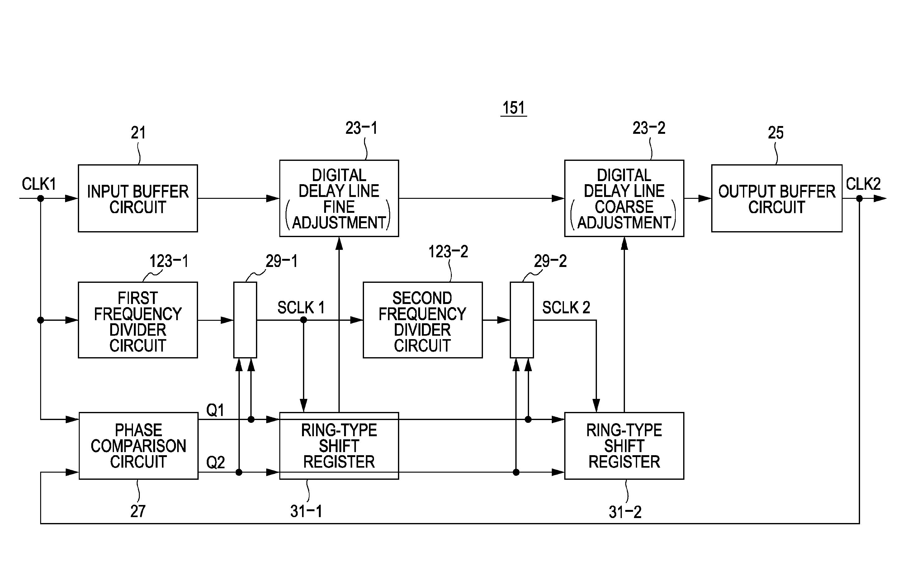
[0137]With this embodiment, a case of frequency division of the input clock CLK1 being used as a shift clock will be described. FIGS. 18 and 19 show a configuration example of clock signal generating circuits with frequency dividing circuits included. FIG. 18 is an example of a clock signal generating circuit 121 where a frequency divider circuit 123 has been added to the first embodiment, and FIG. 19 is an example of a clock signal generating circuit 131 where the frequency divider circuit 123 has been added to the second embodiment.

[0138]Note that frequency division by the frequency divider circuit 123 is optional. In either case, the frequency of the shift clock SCLK can be made lower than the input clock CLK1, so operating margin can be ensured for the ring-type shift registers 31 and 103 by just that much. Consequently, influence on yield can be reduced.


PUM


Abstract

A delay synchronization loop type clock signal generating circuit includes: a digital delay line for delaying a first clock signal and generating a second clock signal; a ring-type shift register for setting the delay time length of the digital delay line by flip-flop output of each stage thereof; and a delay amount control unit for controlling supply of shift clocks to the ring-type shift register, based on phase relation between the first clock signal and the second clock signal.

Description

CROSS REFERENCES TO RELATED APPLICATIONS[0001]The present invention contains subject matter related to Japanese Patent Application JP 2007-314634 filed in the Japanese Patent Office on Dec. 5, 2007, the entire contents of which are incorporated herein by reference.BACKGROUND OF THE INVENTION[0002]1. Field of the Invention[0003]The present invention relates to a delay synchronization loop type signal generating circuit, and in particular, that which is preferably applicable to cases wherein active elements are formed using thin-film formation techniques and printing techniques. The present invention also can serve as a display panel module, an imaging device, and electronic equipment.[0004]2. Description of the Related Art[0005]As of recent, there is demand for high definition display resolution with not only large-screen displays but also middle-to-small range displays as well. Accordingly, higher frequency input clock signals and video signals are being used. For example, with a sy...

Claims


Application Information

Patent Timeline
Patent Type & Authority Patents(United States)
IPC IPC(8): H03L7/00G09G3/20G09G3/36H03K5/131H03K5/14H03K5/15H03L7/081H04N5/66
CPCH03L7/0814H03L7/0818H03L7/10H03L7/0816H03L7/081H03K5/14
Inventor SENDA, MICHIRUMIZUHASHI, HIROSHI
Owner JAPAN DISPLAY WEST
Why Eureka
Try Eureka