Base line restoration circuit

a restoration circuit and base line technology, applied in the direction of low noise amplifiers, particle separator tube details, separation processes, etc., can solve the problems of base line shift dependent, dc coupling of a detector may not be possible, etc., to reduce reduce the noise, cancel or reduce the effect of the detector ac coupling

Inactive Publication Date: 2011-02-08
LECO CORPORATION
View PDF23 Cites 19 Cited by
  • Summary
  • Abstract
  • Description
  • Claims
  • Application Information

AI Technical Summary

Benefits of technology

[0008]In each of these embodiments, the base line restoration for a time-of-flight mass spectrometer is provided to correct for errors introduced by the AC coupling network of an ion detector.

Problems solved by technology

Although this method provides high frequency coupling, the lower frequency components are not transferred to the data collection system resulting in a base line shift this is dependant on output magnitude and duration.
DC coupling of a detector may not be possible due to high voltages present on the detection device.

Method used


Image

  • Base line restoration circuit
  • Base line restoration circuit
  • Base line restoration circuit

Examples


example 1

Integrate and Inject Compensation Current

[0015]In one embodiment, the circuit of FIG. 4 achieves base line correction by injecting a current equal to that which flows due to the built up charge in the detector's AC coupling network of C1, C4 and R6. When the +HV supply is connected to a stiff supply (which is preferable in most cases), C1 is no longer a factor in the time constant. To mimic the response of R6 and C4, the base line restore circuit 20 of FIG. 4 employs a low pass filter R8 and C5 coupled in shunt with the termination resistance R4, the data systems input impedance. The data system could be the input to an analog to digital (A / D) converter or an amplifier stage. C3 is present to block DC current thus preventing run away of the compensation over time. The value of C3 is chosen to be much greater than C5. R1 provides a DC reference and has a resistance which is much greater than that of R8. The voltage measured on C5 is converted to a current by voltage controlled curren...

example 2

Current Driven Integrator Compensator

[0018]A noise performance improvement to the integrate and inject compensation circuit of FIG. 4 can be made by moving the integration function to after the current source. This allows the noise bandwidth of the circuit to be limited by the integration capacitor. A preferred circuit of this type is illustrated in FIG. 6. In this circuit 30, the compensation circuit is connected to the load termination. Transconductance amplifier U1 creates a current at pin 8 that is proportional to the voltage present at pin 3 divided by the resistance present in the emitter (E) circuit. U1's bias current is controlled by R5 which adjusts the internal emitter resistance. This internal resistance added to R3 represents the resistance seen by the emitter circuit for AC signals. In this case, the total AC emitter resistance is adjusted to be 50 Ohms. The DC emitter resistance is much higher eliminating potential lockup of the circuit due to high DC values. The DC em...

example 3

Low Noise Amplifier Base Line Correction

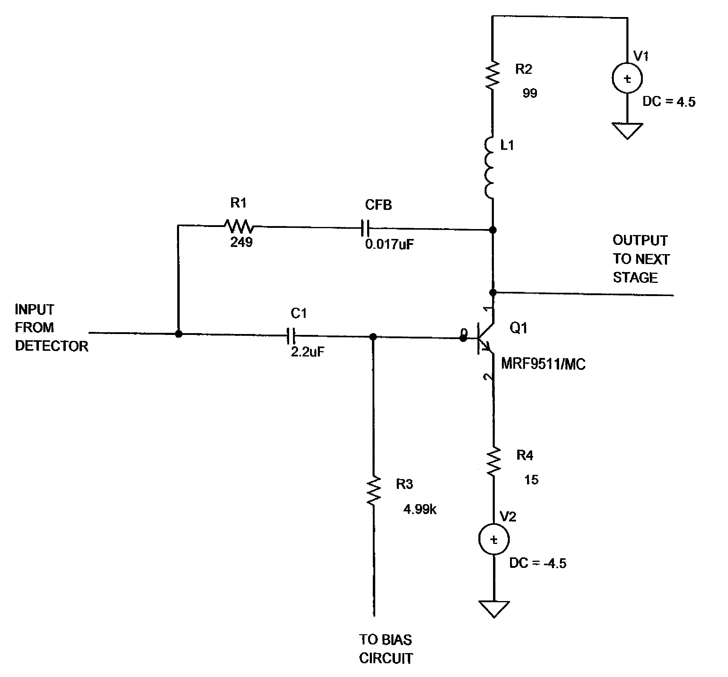
[0021]The previous circuits can be added to an existing data collection system to remove the effects of base line shift caused by AC detector coupling. However, both circuits increase the total system noise due to the added active components. Some data collection electronics include a low noise amplifier circuit to boost the signal level to a value adequate for further analysis. Typical noise levels for this type of preamplifier are specified in the range of 1.5 nV / Hz^0.5. To achieve these noise levels, discrete transistor designs are typically utilized that employ feedback techniques to create the desired 50 Ohm input impedance. Feedback is used since a termination resistor of 50 Ohms will have a noise level of 0.9 nV / Hz^0.5.

[0022]A typical low noise amplifier 40 (FIG. 7) will consist of a low noise RF transistor Q1 which is feed through a large blocking capacitor C1. Feedback is created by R4 in the emitter circuit and R1 in the collector to...


PUM


Abstract

Circuits for correcting base line shift of the detector coupling circuit of a TOFMS provide gain and impedance characteristics that compensate for the AC coupling effect of the detector. In one circuit, base line correction is achieved by injecting a current equal to that which flows due to the buildup charge in the detectors AC coupling network. In another circuit, the current source drives an integrator which is coupled to the signal path to reduce the detector AC coupling effects. In another circuit, a low noise amplifier utilizes a feedback network that reduces the detector AC coupling effects. In yet another circuit, an operational amplifier is employed to reduce the detector AC coupling effects.

Description

CROSS-REFERENCE TO RELATED APPLICATIONS[0001]This application claims priority under 35 U.S.C. §119(e) on U.S. Provisional Application No. 60 / 878,299 entitled Base Line Restoration Circuit, filed on Jan. 3, 2007, by Ted J. Casper, the entire disclosure of which is incorporated herein by reference.BACKGROUND OF THE INVENTION[0002]The present invention relates to circuits that compensate for the base line offset caused by AC coupling of a detection system.[0003]Ion detectors suitable for time-of-flight mass spectroscopy (TOFMS) have become available that allow the data collection system to be at a different potential than the ion detecting device. This allows the ion detector voltages to be optimized for sensitivity and resolution without requiring the output stage of the ion detector to be near ground potential. These detectors use a DC blocking capacitor to couple the electron current from the detector output to the data collection system. An example of this type of detector would be...

Claims


Application Information

Patent Timeline
Patent Type & Authority Patents(United States)
IPC IPC(8): B01D59/44H01J49/00
CPCH01J49/022H01J49/025H03F1/34H03F2200/498H03F2200/156H03F2200/294H03F2200/144
Inventor CASPER, TED J.
Owner LECO CORPORATION
Why Eureka
Try Eureka