Supercharge Your Innovation With Domain-Expert AI Agents!

Nitride semiconductor light-emitting device providing efficient light extraction

a light-emitting device and semiconductor technology, applied in semiconductor devices, basic electric elements, electrical appliances, etc., can solve the problems of disadvantageous deterioration and blackening of transparent conductive films, low contact resistance of electrodes with respect, and limitation of process temperature regions, so as to achieve the effect of improving light extraction efficiency

Active Publication Date: 2011-02-22
SHARP FUKUYAMA LASER CO LTD
View PDF10 Cites 0 Cited by
  • Summary
  • Abstract
  • Description
  • Claims
  • Application Information

AI Technical Summary

Benefits of technology

This configuration significantly increases light extraction efficiency by improving ohmic contact and reducing driving voltage, while maintaining high quantum efficiency and preventing temperature rise.

Problems solved by technology

First, the electrode must have high transmittance with respect to light emitted from an emission layer of the nitride semiconductor light-emitting diode.
Second, the electrode must have sufficient resistance and a sufficient thickness to be capable of sufficiently diffusing an injected current in the plane of the emission layer.
Third, the electrode must have low contact resistance with respect to the p-type nitride semiconductor layer.
In the transparent conductive film of ITO, however, photochemical properties irreversibly change under a high temperature to lower transmittance for visible light, leading to limitation of a temperature region for a process after formation of the transparent conductive film.
Further, the transparent conductive film is disadvantageously deteriorated and blackened when driven with high current density.
In each of the methods disclosed in Japanese Patent Laying-Open Nos. 08-097468 and 11-340509, however, it is difficult to attain excellent ohmic contact by lowering the barrier between the p-type nitride semiconductor layer and the electrode formed on the surface thereof.
In the method disclosed in each of the aforementioned Japanese Patent Laying-Open Nos. 2005-229085, 2005-268601, 2005-268739 and 2006-135311, however, light extraction efficiency is still insufficient.

Method used


Image

  • Nitride semiconductor light-emitting device providing efficient light extraction
  • Nitride semiconductor light-emitting device providing efficient light extraction
  • Nitride semiconductor light-emitting device providing efficient light extraction

Examples


first embodiment

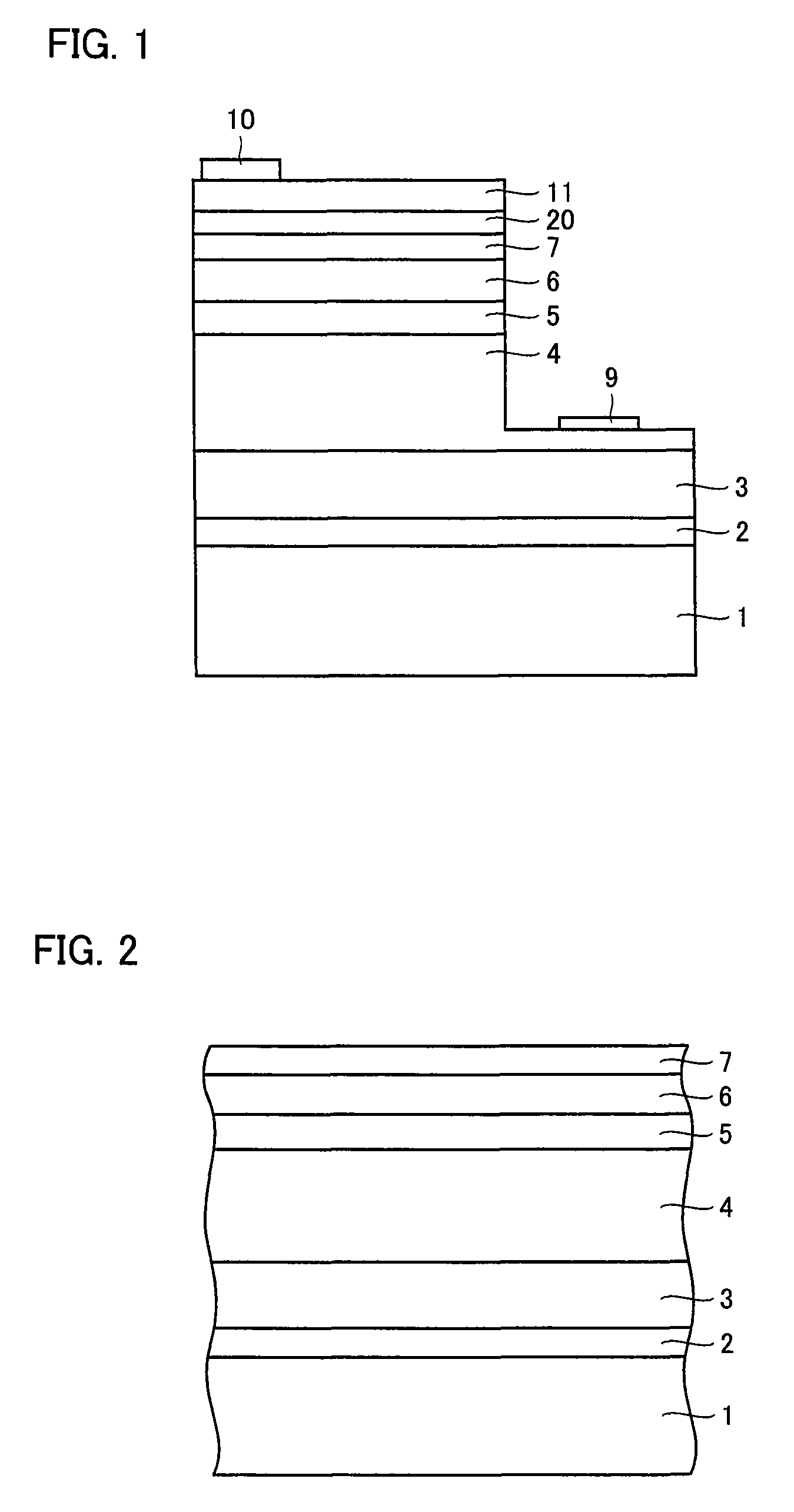
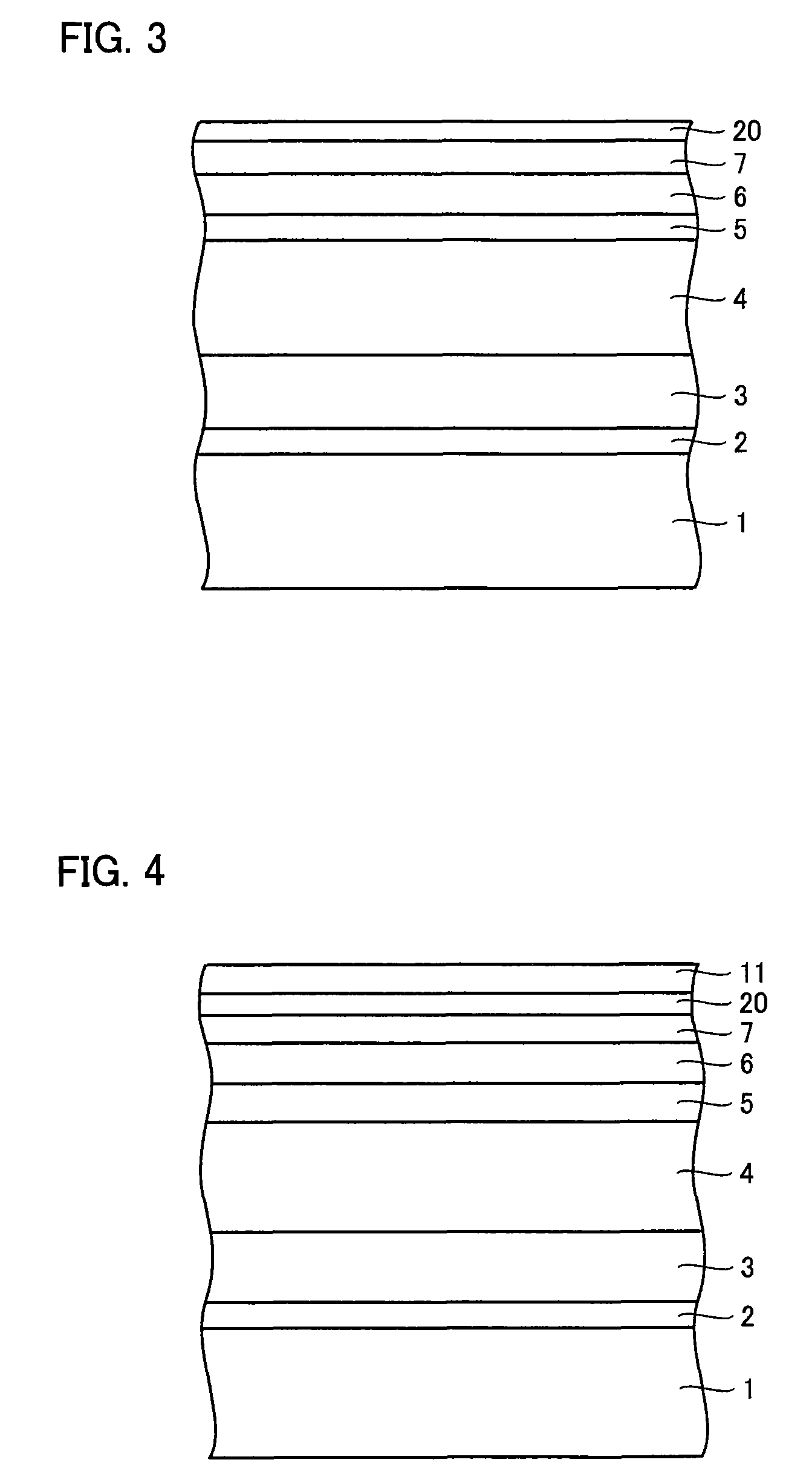
FIG. 1 is a schematic sectional view of an exemplary nitride semiconductor light-emitting diode according to the present invention. In the nitride semiconductor light-emitting diode, a buffer layer 2 of GaN or the like, for example, an n-type nitride semiconductor underlayer 3 of n-type GaN or the like, for example, an n-type nitride semiconductor contact layer 4 of n-type GaN or the like, for example, an emission layer 5 having a multiple quantum well structure obtained by alternately stacking an In0.25Ga0.75N layer and a GaN layer, for example, a p-type nitride semiconductor clad layer 6 of p-type AlGaN or the like, for example, a p-type nitride semiconductor contact layer 7 of p-type GaN or the like, for example, a metal layer 20 of Pd or the like, for example, and a second n-type nitride semiconductor layer 11 of n-type GaN or the like are stacked on a substrate 1 of sapphire or the like, for example, in this order. An n-side pad electrode 9 is formed on the surface of n-type ni...

second embodiment

FIG. 7 is a schematic sectional view of an another exemplary a nitride semiconductor light-emitting diode according to the present invention. The nitride semiconductor light-emitting diode shown in FIG. 7 is characterized in that a semiconductor layer 21 doped with both of an n-type dopant and a p-type dopant is provided between a p-type nitride semiconductor contact layer 7 and a metal layer 20.

Thus, when semiconductor layer 21 doped with both of an n-type dopant and a p-type dopant is provided between p-type nitride semiconductor contact layer 7 and metal layer 20, planarity is increased and crystallinity is improved as compared with a semiconductor layer doped with only a p-type dopant, whereby carriers easily spread in the plane of an emission layer 5, and a nitride semiconductor light-emitting diode having high light extraction efficiency can be obtained.

Semiconductor layer 21 can be formed by a nitride semiconductor layer of InGaN or the like grown by feeding TMG (trimethyl ga...

third embodiment

FIG. 8 is a schematic sectional view of an another exemplary nitride semiconductor light-emitting diode according to the present invention. The nitride semiconductor light-emitting diode shown in FIG. 8 is characterized in that a semiconductor layer 21 doped with both of an n-type dopant and a p-type dopant is provided between a metal layer 20 and a second n-type nitride semiconductor layer 11.

Thus, when semiconductor layer 21 doped with both of an n-type dopant and a p-type dopant is provided between metal layer 20 and second n-type nitride semiconductor layer 11, a potential drop between a p-type nitride semiconductor contact layer 7 and second n-type nitride semiconductor layer 11 can be reduced and increase in driving voltage for the nitride semiconductor light-emitting diode can be suppressed. While the reason for this is not obvious, it is inferred that this is because carriers move between the valence band of p-type nitride semiconductor contact layer 7 and the conduction ban...


PUM

PropertyMeasurementUnit
band gapaaaaaaaaaa
band gap energyaaaaaaaaaa
light extraction efficiencyaaaaaaaaaa

Abstract

A nitride semiconductor light-emitting device comprises a substrate, and a first n-type nitride semiconductor layer, an emission layer, a p-type nitride semiconductor layer, a metal layer and a second n-type nitride semiconductor layer stacked on the substrate successively from the side closer to the substrate, with an electrode provided on the surface of the second n-type nitride semiconductor layer or above the surface of the second n-type nitride semiconductor layer. The metal layer is preferably made of a hydrogen-storage alloy.

Description

This nonprovisional application is based on Japanese Patent Application No. 2007-019647 filed with the Japan Patent Office on Jan. 30, 2007, the entire contents of which are hereby incorporated by reference.BACKGROUND OF THE INVENTION1. Field of the InventionThe present invention relates to a nitride semiconductor light-emitting device, and more particularly, it relates to a nitride semiconductor light-emitting device improvable in light extraction efficiency.2. Description of the Background ArtIn the structure of a conventional nitride semiconductor light-emitting diode, serving as a nitride semiconductor light-emitting device, having a p-type nitride semiconductor layer forming a light extraction side, an electrode formed on the surface of the p-type nitride semiconductor layer must satisfy the following three conditions:First, the electrode must have high transmittance with respect to light emitted from an emission layer of the nitride semiconductor light-emitting diode.Second, t...

Claims


Application Information

Patent Timeline
Patent Type & Authority Patents(United States)
IPC IPC(8): H01L33/00H01L33/32H01L33/40H01L33/06
CPCH01L33/40H01L33/14H01L33/32
Inventor OGAWA, ATSUSHIAIOI, AKIOKOMADA, SATOSHINAKATSU, HIROSHI
Owner SHARP FUKUYAMA LASER CO LTD
Features
  • R&D
  • Intellectual Property
  • Life Sciences
  • Materials
  • Tech Scout
  • Unparalleled Data Quality
  • Higher Quality Content
  • 60% Fewer Hallucinations
Learn More