Nitride semiconductor light-emitting device
a light-emitting device and semiconductor technology, applied in the direction of semiconductor devices, basic electric elements, electrical appliances, etc., can solve the problems of disadvantageous deterioration and blackening of transparent conductive films, low contact resistance of electrodes with respect, etc., to achieve the effect of improving light extraction efficiency
- Summary
- Abstract
- Description
- Claims
- Application Information
AI Technical Summary
Benefits of technology
Problems solved by technology
Method used
Image

Examples
first embodiment
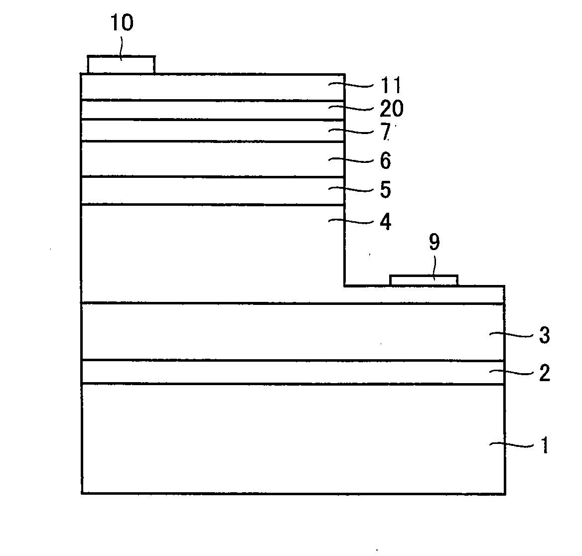
[0032]FIG. 1 is a schematic sectional view of an exemplary nitride semiconductor light-emitting diode according to the present invention. In the nitride semiconductor light-emitting diode, a buffer layer 2 of GaN or the like, for example, an n-type nitride semiconductor underlayer 3 of n-type GaN or the like, for example, an n-type nitride semiconductor contact layer 4 of n-type GaN or the like, for example, an emission layer 5 having a multiple quantum well structure obtained by alternately stacking an In0.25Ga0.75N layer and a GaN layer, for example, a p-type nitride semiconductor clad layer 6 of p-type AlGaN or the like, for example, a p-type nitride semiconductor contact layer 7 of p-type GaN or the like, for example, a metal layer 20 of Pd or the like, for example, and a second n-type nitride semiconductor layer 11 of n-type GaN or the like are stacked on a substrate 1 of sapphire or the like, for example, in this order. An n-side pad electrode 9 is formed on the surface of n-t...
second embodiment
[0048]FIG. 7 is a schematic sectional view of an another exemplary a nitride semiconductor light-emitting diode according to the present invention. The nitride semiconductor light-emitting diode shown in FIG. 7 is characterized in that a semiconductor layer 21 doped with both of an n-type dopant and a p-type dopant is provided between a p-type nitride semiconductor contact layer 7 and a metal layer 20.
[0049]Thus, when semiconductor layer 21 doped with both of an n-type dopant and a p-type dopant is provided between p-type nitride semiconductor contact layer 7 and metal layer 20, planarity is increased and crystallinity is improved as compared with a semiconductor layer doped with only a p-type dopant, whereby carriers easily spread in the plane of an emission layer 5, and a nitride semiconductor light-emitting diode having high light extraction efficiency can be obtained.
[0050]Semiconductor layer 21 can be formed by a nitride semiconductor layer of InGaN or the like grown by feeding...
third embodiment
[0052]FIG. 8 is a schematic sectional view of an another exemplary nitride semiconductor light-emitting diode according to the present invention. The nitride semiconductor light-emitting diode shown in FIG. 8 is characterized in that a semiconductor layer 21 doped with both of an n-type dopant and a p-type dopant is provided between a metal layer 20 and a second n-type nitride semiconductor layer 11.
[0053]Thus, when semiconductor layer 21 doped with both of an n-type dopant and a p-type dopant is provided between metal layer 20 and second n-type nitride semiconductor layer 11, a potential drop between a p-type nitride semiconductor contact layer 7 and second n-type nitride semiconductor layer 11 can be reduced and increase in driving voltage for the nitride semiconductor light-emitting diode can be suppressed. While the reason for this is not obvious, it is inferred that this is because carriers move between the valence band of p-type nitride semiconductor contact layer 7 and the co...
PUM
| Property | Measurement | Unit |
|---|---|---|
| semiconductor | aaaaa | aaaaa |
| band gap | aaaaa | aaaaa |
| band gap energy | aaaaa | aaaaa |
Abstract
Description
Claims
Application Information
 - R&D
- Intellectual Property
- Life Sciences
- Materials
- Tech Scout
- Unparalleled Data Quality
- Higher Quality Content
- 60% Fewer Hallucinations
Browse by: Latest US Patents, China's latest patents, Technical Efficacy Thesaurus, Application Domain, Technology Topic, Popular Technical Reports.
© 2025 PatSnap. All rights reserved.Legal|Privacy policy|Modern Slavery Act Transparency Statement|Sitemap|About US| Contact US: help@patsnap.com