Statistical design closure

a technology of statistical design and closure, applied in the field of statistical design closure, can solve the problems of long design closure run of large circuit design, unpredictable ability to estimate how much and how long resources will be consumed closing the design of a large circuit, and complex design closure of current chip design, so as to avoid spending resources on tasks, optimize resource use, and focus work

Active Publication Date: 2011-02-22
BELL SEMICON LLC
View PDF2 Cites 99 Cited by
  • Summary
  • Abstract
  • Description
  • Claims
  • Application Information

AI Technical Summary

Benefits of technology

[0006]The objects, features and advantages of the present invention include providing a statistical design closure that may (i) achieve an intended chip yield, (ii) optimize the use of resources, (iii) focus the work on important tasks, (iv) avoid spending resources on tasks that achieve little benefit, (v) minimize over-constraining the design in anticipation of unknowns, (vi) minimize the margins added to the design to account for the unknowns and / or (vii) produce fast turn-around-times.

Problems solved by technology

Design closure of current chip designs has become complex.
The ability to estimate how long and how much resources will be consumed closing the design of a large circuit has become unpredictable in the early phase of the design closure.
Design closure runs of the large circuits are taking a long time.
Furthermore, the projects are not always staffed correctly.
As a result, scheduling remains unpredictable and the circuits are often delivered late.
Unfortunately, the existing solutions can have drawbacks.
Having more engineers assigned to the projects does not always result in a faster turn around time.
Furthermore, conducting several design closure runs on the same chip in parallel using several machines is inefficient.

Method used


Image

  • Statistical design closure
  • Statistical design closure
  • Statistical design closure

Examples


Embodiment Construction

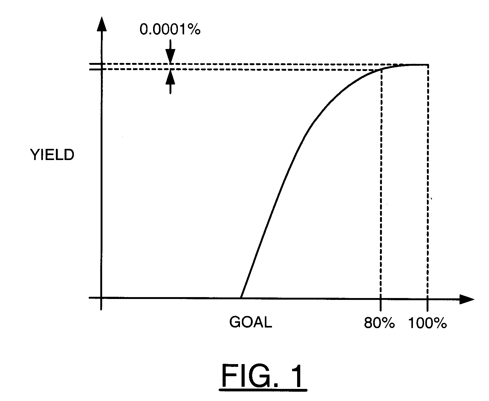
[0013]Design closure generally contains a design process comprising steps of synthesis, floorplanning, placement, routing and other steps. A foundation of statistical design closure may be that many variables and variations of processes, design flows and methodologies may impact a final behavior of a chip. In common design closures, the goal of a single design closure step is either met or not. However, the individual design engineers and / or program managers do not know what impact each of the variables and variations actually has on the overall process.

[0014]Referring to FIG. 1, a diagram of an example yield graph is shown. The graph may express a statistical yield (e.g., probability) as a function of achieving a defined goal. In the example shown, a 20% less aggressive design closure in the timing (e.g., 80% of the goal) of a particular structure may only impact the final chip yield (e.g., working parts) by 0.0001%. Valuable resource might be focusing on the wrong part of design c...


PUM


Abstract

A method of statistical design closure is disclosed. The method generally includes the steps of (A) reading statistical data from a database, the statistical data defining a plurality of chip yield improvements, one of the chip yield improvements in each one of a plurality of design closure categories respectively, the chip yield improvements capturing historically trends based on a plurality of previous projects, (B) calculating a plurality of targets of a current design closure project based on the statistical data, one of the targets in each one of the design closure categories respectively and (C) generating a resource report to a user that indicates a plurality of resources expected to be used the current design closure project.

Description

FIELD OF THE INVENTION[0001]The present invention relates to chip design techniques generally and, more particularly, to a statistical design closure.BACKGROUND OF THE INVENTION[0002]Design closure of current chip designs has become complex. The ability to estimate how long and how much resources will be consumed closing the design of a large circuit has become unpredictable in the early phase of the design closure. Design closure runs of the large circuits are taking a long time. Margins are being used to handle risks of not being able to close timing. Constraints are either being merged or used in multiple modes. Furthermore, the projects are not always staffed correctly. As a result, scheduling remains unpredictable and the circuits are often delivered late.[0003]To account for the unpredictability, many projects add margins or over-constraining the design in early phases. Some projects use multiple runs and multiple loops to reach design closure. More licenses and machines have ...

Claims


Application Information

Patent Timeline
Patent Type & Authority Patents(United States)
IPC IPC(8): G06F17/50
CPCG06F17/5022G06F2217/10G06F30/33G06F2111/08
Inventor LAHNER, JUERGEN K.BALASUBRAMANIAN, BALAMURUGANCHATURVEDULA, KAVITHA
Owner BELL SEMICON LLC
Why Eureka
Try Eureka