Integrated circuit (IC) design method, system and program product

a technology of integrated circuits and design methods, applied in cad circuit design, program control, instruments, etc., can solve the problems of reducing chip yield, increasing the cost of generating complex masks, and chip defects, so as to improve the efficiency of layout data preparation, reduce the cost and risk of layout generation, and improve the effect of ics

Inactive Publication Date: 2011-03-01
GLOBALFOUNDRIES INC
View PDF6 Cites 8 Cited by
  • Summary
  • Abstract
  • Description
  • Claims
  • Application Information

AI Technical Summary

Benefits of technology

[0013]It is yet another purpose of the invention to reduce the cost and risk of layout generation and layout checking of chips with circuits that include features that may be process dependent and require special treatment, e.g., feature-specific design ground rules and checking;
[0014]It is yet another purpose of the invention to improve the efficiency of layout data preparation in designs with circuits that include process dependent features that require feature-specific design ground rules and checking;
[0015]It is yet another purpose of the invention to improve the efficiency of ICs that include special case circuits that include features that may be process dependent and require special treatment, and are represented in gridded glyph geometric objects (L3GO) format.

Problems solved by technology

Mask errors translate to chip errors that can cause chip defects.
Even the resulting defective chips are functional, the design may be marginal, reducing chip yield.
Consequently, as these masks become increasingly complex, generating complex masks has become more expensive, requiring increased design creativity and effort for lithographic patterning and for manipulating the design data flow to manufacturing.
Thus, manufacturing costs and risks inherent in making these complex patterns have made ineffective and obsoleted some state of the art layout methodologies and computer-aided design tools that had otherwise been used.
However, Cohn et al. has not yet been applied, effectively, to circuits with features that may be process dependent and require special treatment, e.g., feature-specific design ground rules and checking.
Typically, such an ad-hoc approach results in choosing irregular design shapes that are not easily represented in L3GO format.
Consequently, insuring chip-wide compliance with these complicated feature-specific rules has reduced productivity.
In addition to designer effort in designing to and verifying compliance with (checking) regular ground rules, for designers using special case cells (i.e., with these special case circuits), design and compliance is even more complicated and time consuming.
Not only have these feature-specific rules complicated ground rule checker coding, for example, ground rule checker results have been complicated too and are difficult designers to understand.
If one cannot understand the ground rule checker results, one cannot identify and fix violations.
Moreover, these complicated rules have hampered design improvements from checking feedback, e.g., to adjust a design as process learning proceeds.

Method used


Image

  • Integrated circuit (IC) design method, system and program product
  • Integrated circuit (IC) design method, system and program product
  • Integrated circuit (IC) design method, system and program product

Examples


Embodiment Construction

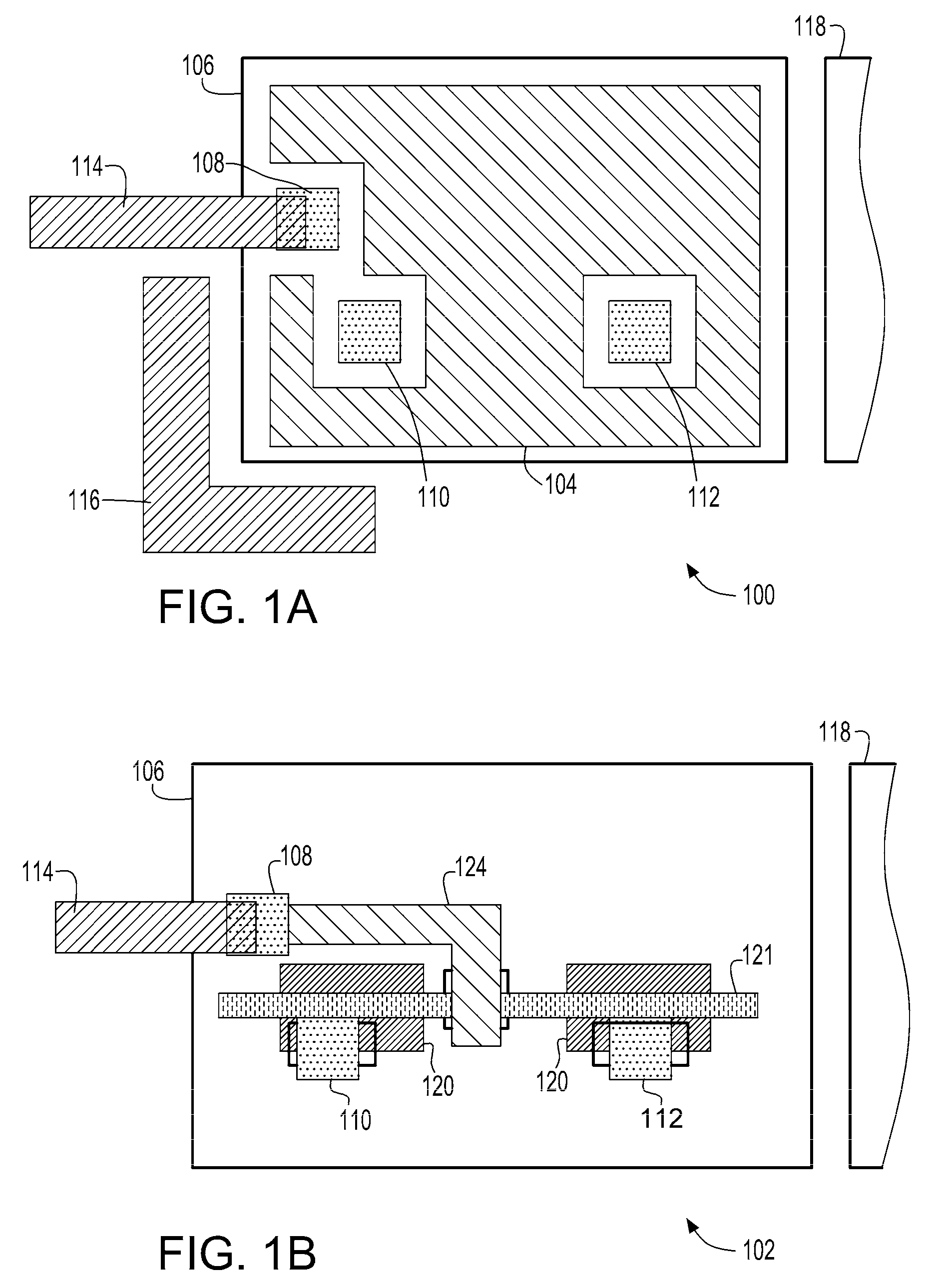
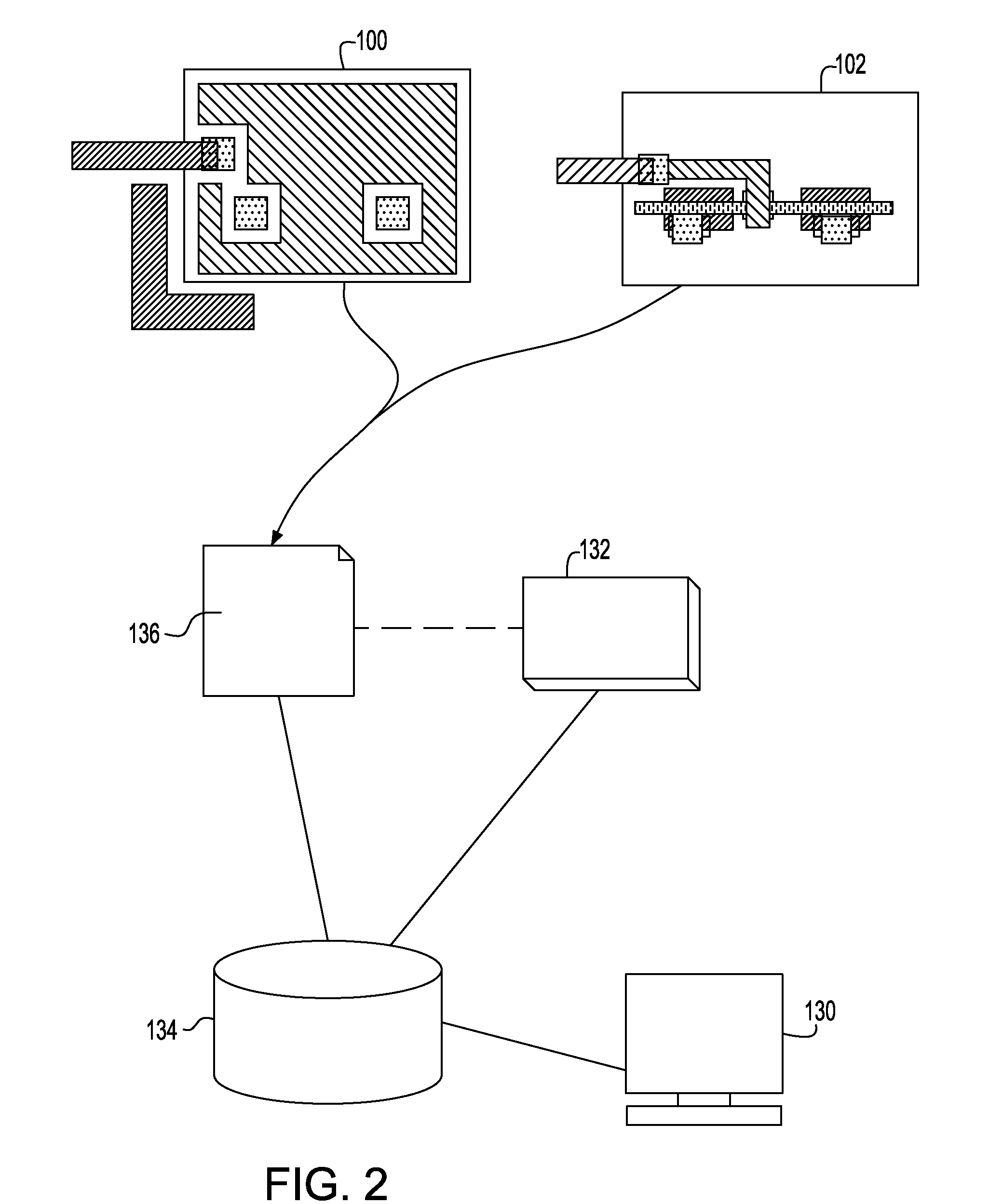
[0021]Turning now to the drawings and, more particularly, FIGS. 1A-B show an example of a dual representation100, 102 of a special case cell, according to a preferred embodiment of the present invention. As used herein, a special case cell includes features that may be process dependent and that require special treatment, e.g., features-specific ground rules and checking. Thus special case cells include, for example only, Static Random Access Memory (SRAM) cells and decoupling capacitors, body contacts, diodes, polysilicon resistors, fuses, or bonding pads, e.g., Controlled Collapse Chip Connections (C4s). This list of special case cells is for example only and not intended as a limitation.

[0022]Preferably in this example, the special case cell is in an integrated circuit (IC) chip design in a gridded glyph geometric objects (L3GO) format, such as is described in U.S. Pat. No. 7,536,664, “Physical Design System And Method” to Cohn et al., assigned to the assignee of the present inve...


PUM


Abstract

A method of integrated circuit (IC) design, an IC design system and computer program product therefore, e.g., for L3GO designs. Special case cells are cells that represent specialized, process dependent components and are provided as dual representation cells with an internal view and external view. The external view is high level abstract representation that includes access pins, boundary and possible blocking shapes / layers and optionally, parameterizations. Each external view includes cell to cell spacing rules and connecting and blocking / keepout rules for placement and routing. The internal representation or, internal view includes regular shapes forming cell components and defining cell construction details and are ground rule clean by construction or verified by simulation or hardware.

Description

CROSS REFERENCE TO RELATED APPLICATION[0001]The present invention is related to U.S. Pat. No. 7,536,664, entitled “PHYSICAL DESIGN SYSTEM AND METHOD” to Cohn et al., published as US 2006 / 0036977 Al, filed Aug. 12, 2004 and published Feb. 16, 2006, and to U.S. application Ser. No. 12 / 047,566, entitled “GRIDDED GLYPH GEOMETRIC OBJECTS (L3GO) DESIGN METHOD” to Lavin et al., filed coincident herewith, all assigned to the assignee of the present invention.BACKGROUND OF THE INVENTION[0002]1. Field of the Invention[0003]The present invention is related to integrated circuit (IC) and chip design systems and more particularly to computer aided design (CAD) systems for designing ICs and IC chips.[0004]2. Background Description[0005]A typical integrated circuit (IC) chip includes a stack of several sequentially formed layers of shapes. Each layer is stacked or overlaid on a prior layer and patterned to form the shapes that define devices (e.g., field effect transistors (FETs)) and wires that c...

Claims


Application Information

Patent Timeline
Patent Type & Authority Patents(United States)
IPC IPC(8): G06F17/50
CPCG06F17/5068G06F30/39
Inventor CULP, JAMES A.NORTHROP, GREGORY A.YIN, MING
Owner GLOBALFOUNDRIES INC
Why Eureka
Try Eureka