

Optical switching element and photoaddressable display medium using the same
a technology of optical switching and display medium, which is applied in the direction of optics, optical light guides, instruments, etc., can solve the problems of poor performance of optical switching generally used in sid, insufficient switching performance in low electric field, and inability to achieve good on/off driving performance, the effect of improving the optical switching function
- Summary
- Abstract
- Description
- Claims
- Application Information
AI Technical Summary
Benefits of technology
Problems solved by technology
Method used
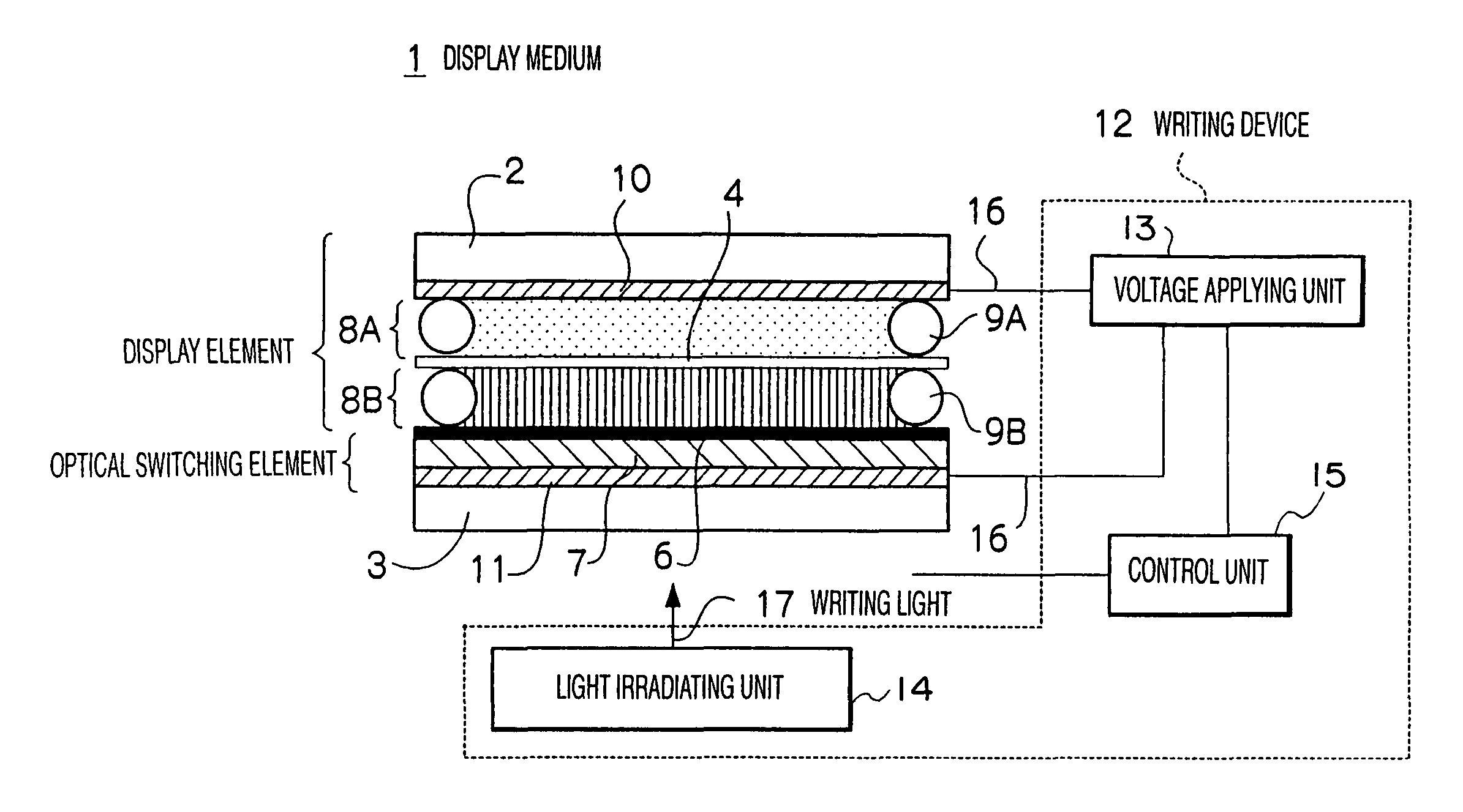
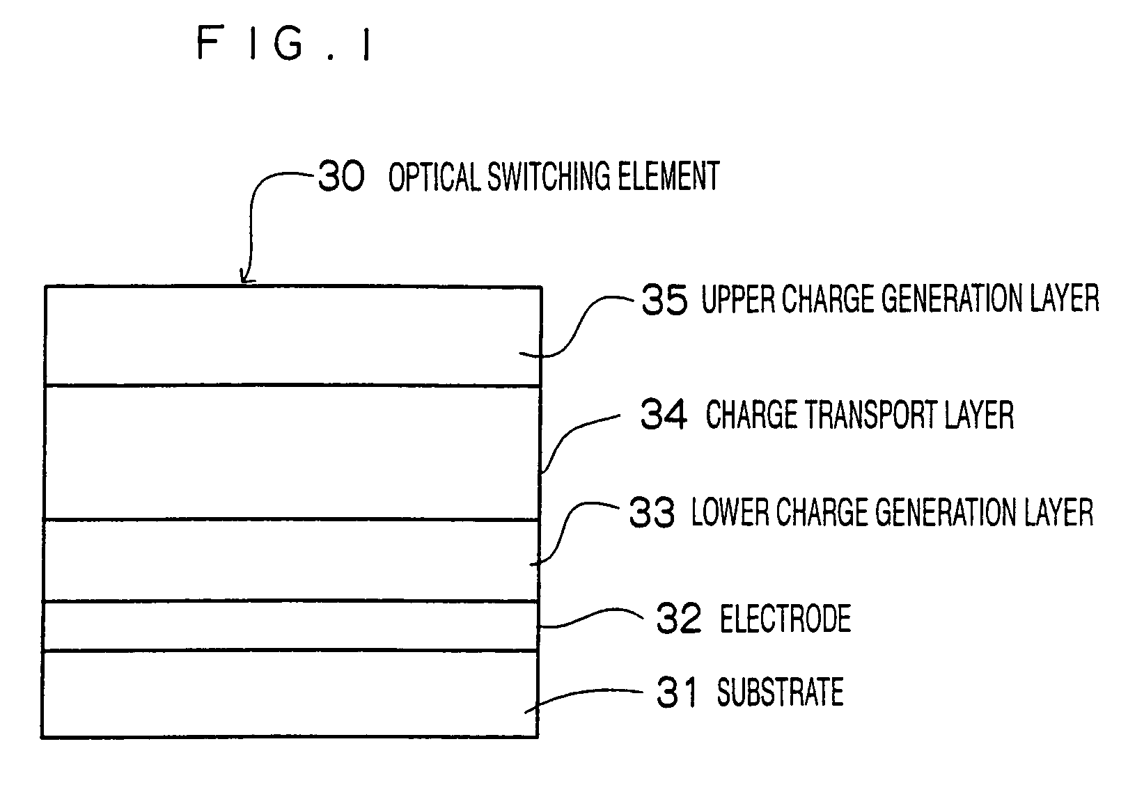
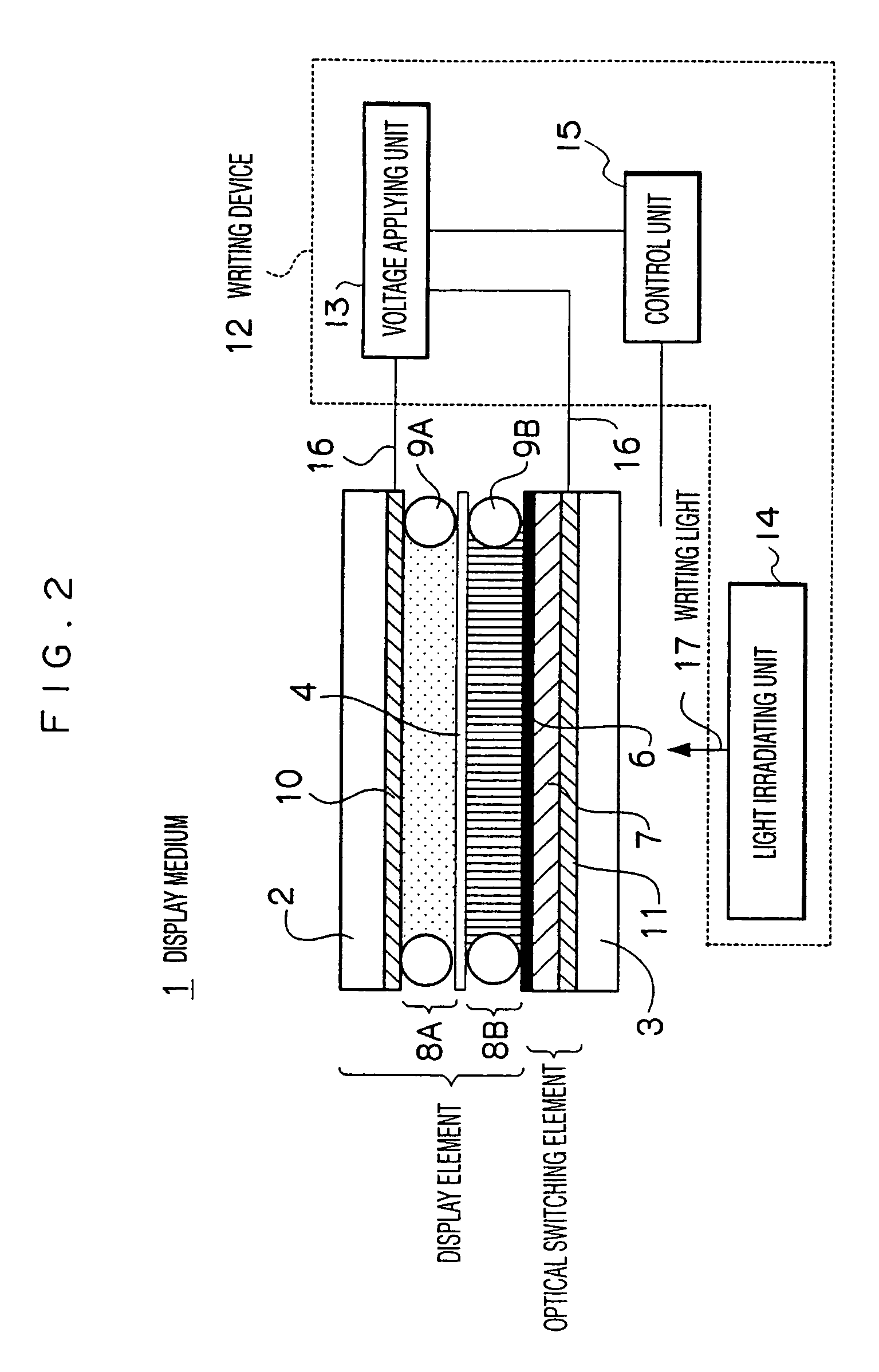
Image

Examples
example 1
[0143]In the process of forming a charge transport layer, monochlorobenzene was used as a solvent, and a polycarbonate resin manufactured by Mitsubishi Gas Chemical Company, Inc. was used as a binder. The charge transporting material having the following structure (Compound 18) was used, and the loading, i.e. the ratio of the charge transporting material in the solid contents, was set at 60% by weight. A solution with a concentration of 15% was prepared.
[0144]
[0145]In a solution for forming a charge generation layer, chlorogallium phthalocyanine was used as the charge generating material. Polyvinyl butyral was used as a binder for it and dispersed into a 1-butanol solution by paint shake. The solid content of the chlorogallium phthalocyanine was set at 60% by weight, and that of the polyvinyl butyral was set at 40% by weight. The solvent concentration was set at 4% SC.
[0146]The resulting solutions were used to form an optical switching element as shown below.
[0147]The solution for t...
example 2
[0149]The process of Example 1 was used to form an optical switching element except that the charge transporting material used had the structure as shown below (Compound 6) and that gallium phthalocyanine was used as the charge generating material.
[0150]
example 3
[0151]The process of Example 1 was used to form an optical switching element except that the charge transporting material used was Compound 6 as shown above and that hydroxyphthalocyanine was used as the charge generating material.
PUM
 Abstract
Description
Claims
Application Information