Separate confinement heterostructure with asymmetric structure and composition
- Summary
- Abstract
- Description
- Claims
- Application Information
AI Technical Summary
Benefits of technology
Problems solved by technology
Method used
Image

Examples
Example
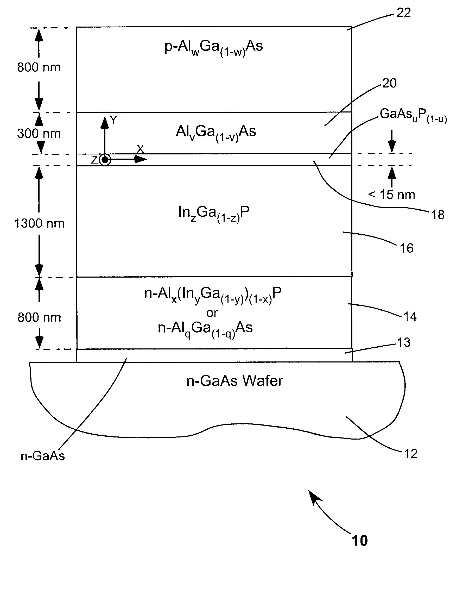
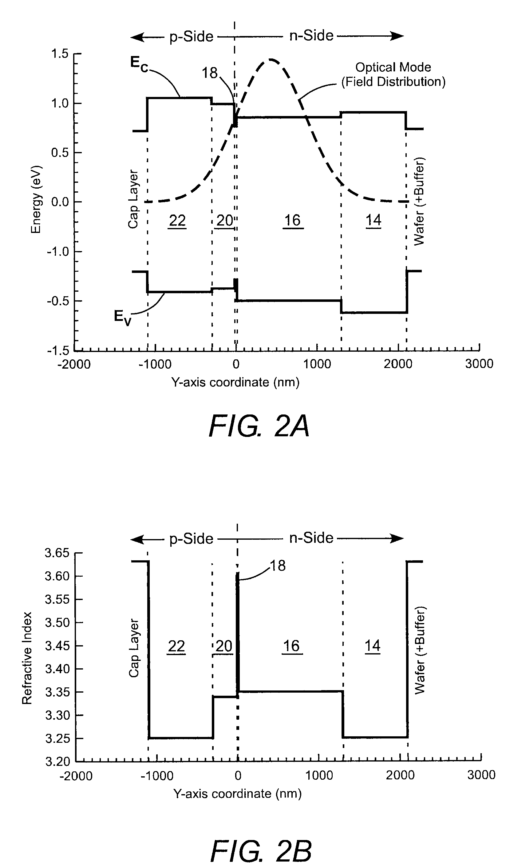
[0013]Referring now to the drawings, wherein like components are designated by like reference numerals, FIG. 1 schematically illustrates a preferred embodiment 10 of a separate confinement heterostructure in accordance with the present invention. The heterostructure is epitaxially grown on an n-doped gallium arsenide wafer (substrate) 12. In the description of the heterostructure below it is assumed that the emission-wavelength of the heterostructure will be about 808 nanometers (nm). This, of course, is just one example, and the emission wavelength and other details of the example should not be considered as limiting the present invention. The fast-axis and slow-axis of the heterostructure are arbitrarily designated as the Y-axis and the Y-axis. The propagation axis (emission direction) is designated as the Z-axis, perpendicular to the plane of the drawing.
[0014]The heterostructure includes a first cladding layer 14 preferably of n-doped aluminum indium gallium phosphide (abbreviat...
PUM
 Abstract
Description
Claims
Application Information
 - R&D Engineer
- R&D Manager
- IP Professional
- Industry Leading Data Capabilities
- Powerful AI technology
- Patent DNA Extraction
Browse by: Latest US Patents, China's latest patents, Technical Efficacy Thesaurus, Application Domain, Technology Topic.
© 2024 PatSnap. All rights reserved.Legal|Privacy policy|Modern Slavery Act Transparency Statement|Sitemap