Thin P-type gallium nitride and aluminum gallium nitride electron-blocking layer free gallium nitride-based light emitting diodes

a light-emitting diode, aluminum gallium nitride technology, applied in the direction of semiconductor/solid-state device manufacturing, electrical apparatus, semiconductor devices, etc., can solve the problem of reducing the absorption of light emitted from the quantum well region, and achieve the effect of reducing the absorption of light emitted and series-resistan

Inactive Publication Date: 2011-10-25
RGT UNIV OF CALIFORNIA
View PDF5 Cites 5 Cited by
  • Summary
  • Abstract
  • Description
  • Claims
  • Application Information

AI Technical Summary

Benefits of technology

[0017]To overcome the limitations in the prior art described above, and to overcome other limitations that will become apparent upon reading and understanding the present invention, the present invention comprises of a novel approach for producing a GaN-based semi-polar-oriented light emitting diode (LED) that contains a thin (i.e. <100 nanometers (nm)) p-type GaN layer and no AlGaN electron-blocking layer (EBL). In the preferred embodiment, freestanding semi-polar (10-1-1) GaN is used as the substrate for the LED. This invention offers several advantages over the existing semi-polar LEDs. First of all, the thin p-type GaN layer and AlGaN EBL free designs can lower series-resistance and thus the operating voltage of a GaN-based LED. Additionally, the thin p-type GaN layer may reduce the absorption of light emitted from the quantum well region. Furthermore, the hole-carrier injection efficiency is likely to benefit from the removal of the AlGaN EBL.
[0020]The LED of the present invention may have a higher luminous efficiency, crystal quality, hole injection efficiency, lower series-resistance, operating voltage, and light absorption as compared to an LED comprising a separate AlGaN blocking layer and thicker p-type layer.

Problems solved by technology

Additionally, the thin p-type GaN layer may reduce the absorption of light emitted from the quantum well region.

Method used


Image

  • Thin P-type gallium nitride and aluminum gallium nitride electron-blocking layer free gallium nitride-based light emitting diodes
  • Thin P-type gallium nitride and aluminum gallium nitride electron-blocking layer free gallium nitride-based light emitting diodes
  • Thin P-type gallium nitride and aluminum gallium nitride electron-blocking layer free gallium nitride-based light emitting diodes

Examples


Embodiment Construction

[0028]In the following description of the preferred embodiment, reference is made to the accompanying drawings which form a part hereof, and in which is shown by way of illustration a specific embodiment in which the invention may be practiced. It is to be understood that other embodiments may be utilized and structural changes may be made without departing from the scope of the present invention.

[0029]Overview

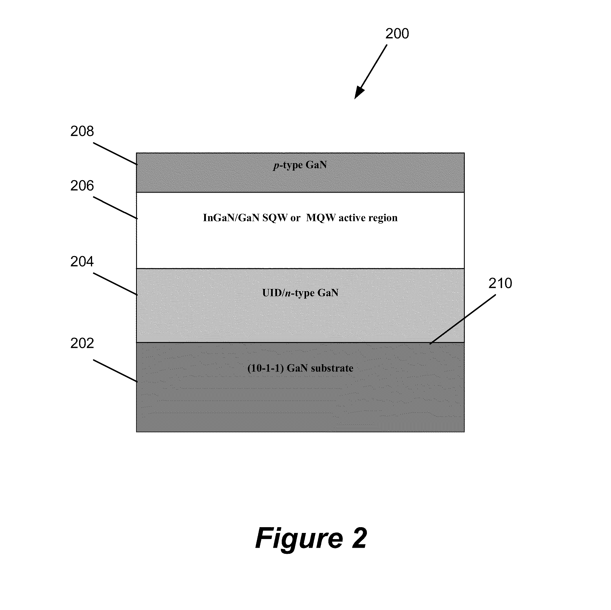
[0030]The purpose of this invention is to generate semi-polar-oriented GaN-based LEDs with improved performance and manufacturability. The proposed device will typically be used as an optical source for various display, illumination, and solid-state lighting applications.

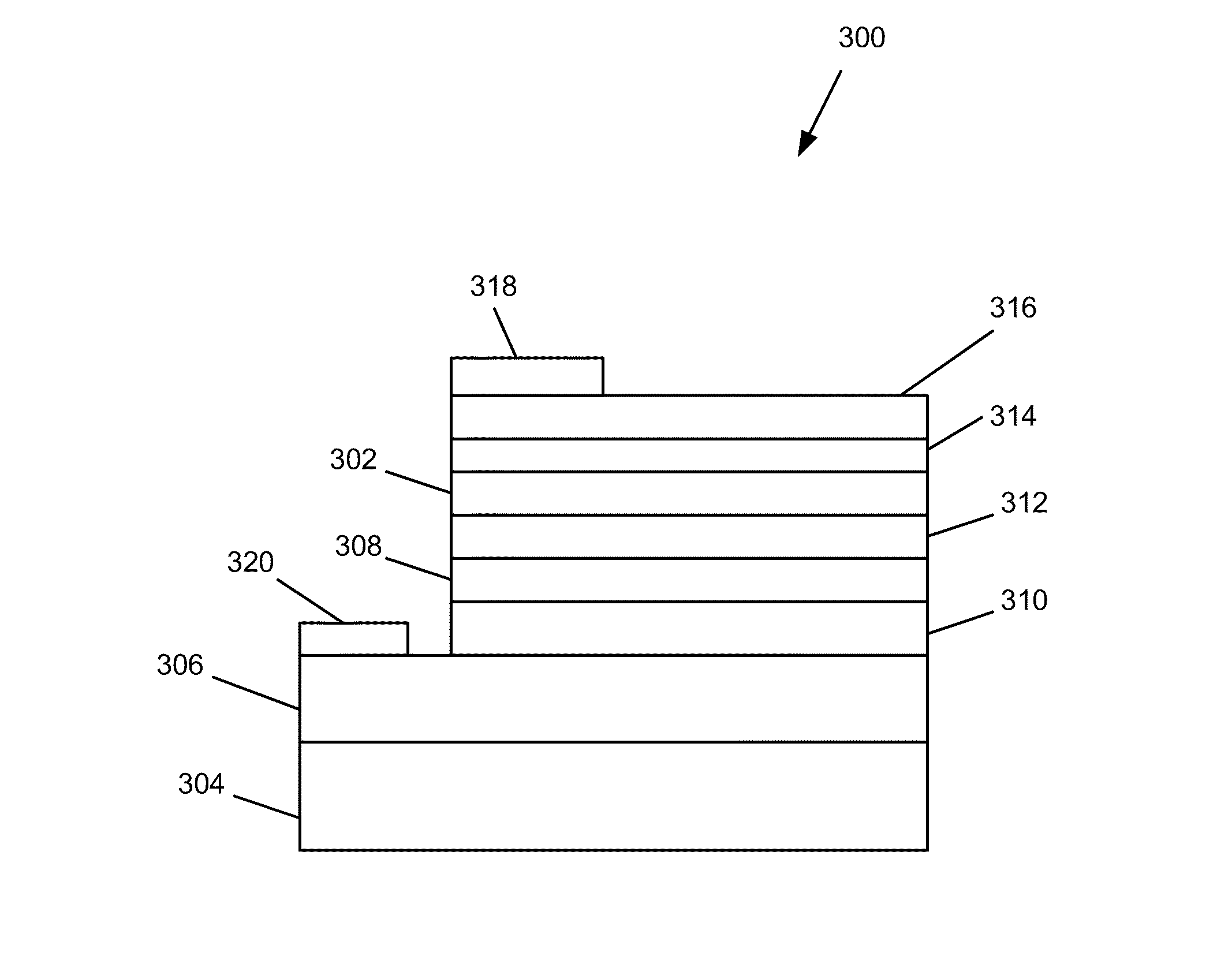
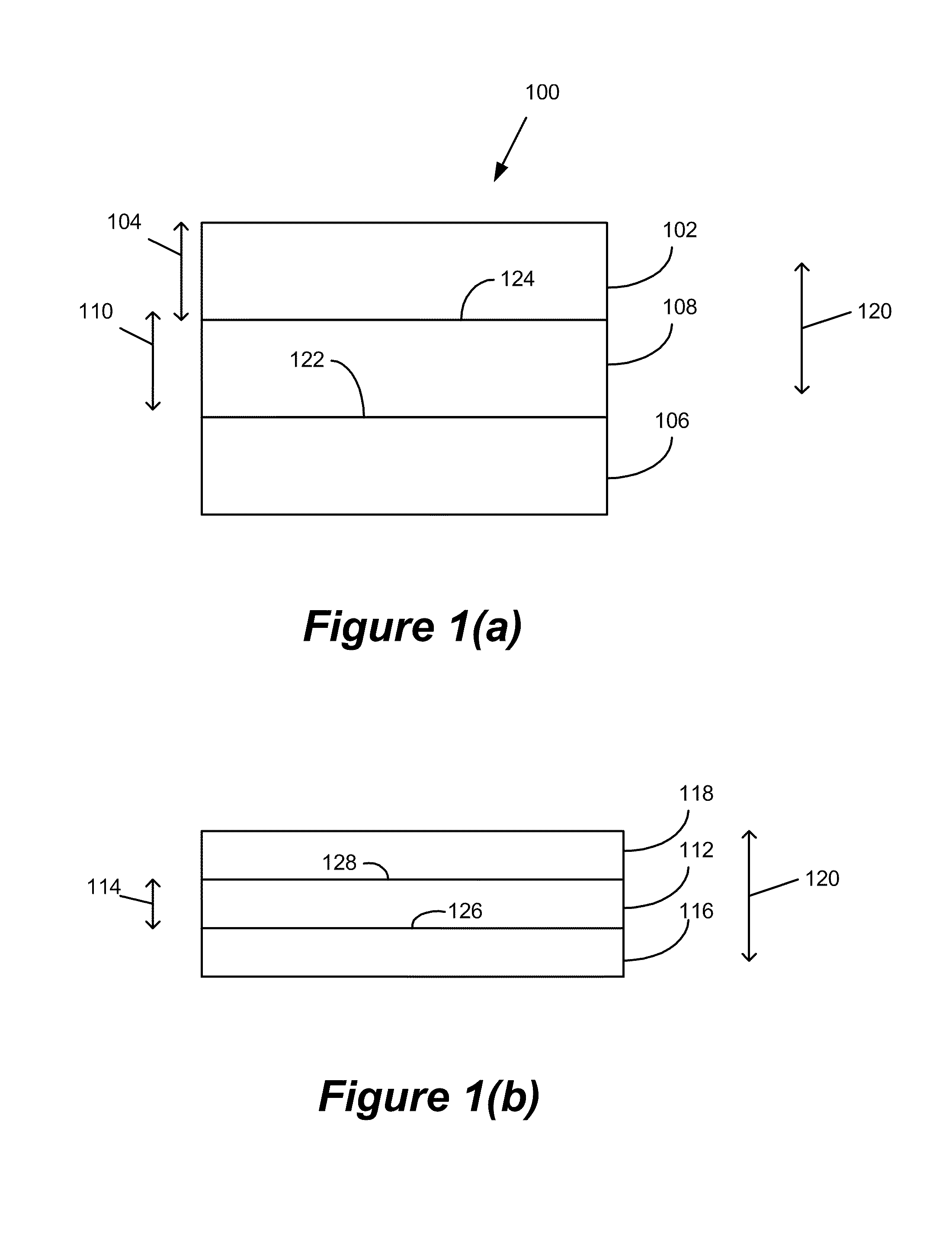
[0031]The realization of thin p-type GaN and AlGaN EBL free LED structures would potentially allow for multiple advances in the manufacturability of GaN-based LEDs (because this invention further simplifies LED epitaxial structure) and yield devices with reduced voltage operation and higher crystal quality. Th...


PUM


Abstract

A light emitting diode (LED) having a p-type layer having a thickness of 100 nm or less, an n-type layer, and an active layer, positioned between the p-type layer and the n-type layer, for emitting light, wherein the LED does not include a separate electron blocking layer.

Description

CROSS-REFERENCE TO RELATED APPLICATIONS[0001]This application claims the benefit under 35 U.S.C. Section 119(e) of co-pending and commonly-assigned U.S. Provisional Application Ser. No. 61 / 111,642 filed on Nov. 5, 2008, by Hong Zhong, Anurag Tyagi, James S. Speck, Steven P. DenBaars, and Shuji Nakamura, entitled “THIN P-TYPE GALLIUM NITRIDE AND ALUMINUM GALLIUM NITRIDE ELECTRON-BLOCKING LAYER FREE GALLIUM NITRIDE-BASED LIGHT EMITTING DIODES,” which application is incorporated by reference herein.[0002]This application is related to the following co-pending and commonly-assigned U.S. patent applications:[0003]U.S. Utility patent application Ser. No. 12 / 370,479, filed on Feb. 12, 2009, by Arpan Chakraborty, Benjamin A. Haskell, Stacia Keller, James S. Speck, Steven P. DenBaars, Shuji Nakamura and Umesh K. Mishra, entitled “FABRICATION OF NONPOLAR INDIUM GALLIUM NITRIDE THIN FILMS, HETEROSTRUCTURES AND DEVICES BY METALORGANIC CHEMICAL VAPOR DEPOSITION,” which application is a continuat...

Claims


Application Information

Patent Timeline
Patent Type & Authority Patents(United States)
IPC IPC(8): H01L29/06H01L31/00
CPCH01L33/02H01L33/18H01L33/16H01L33/32
Inventor ZHONG, HONGTYAGI, ANURAGSPECK, JAMES S.DENBAARS, STEVEN P.NAKAMURA, SHUJI
Owner RGT UNIV OF CALIFORNIA
Why Eureka
Try Eureka