Main-gate-free and high-efficiency back-contact solar cell module, main-gate-free and high-efficiency back-contact solar cell assembly, and preparation process thereof

a solar cell and back-contact technology, applied in the field of solar cells, can solve the problems of reducing the effective light-receiving area affecting the efficiency of the solar cell, so as to reduce the electron collection distance, reduce the series resistance of the assembly, and simplify the preparation process

Active Publication Date: 2017-08-03
JOLYWOOD SUZHOU SUNWATT
View PDF9 Cites 42 Cited by
  • Summary
  • Abstract
  • Description
  • Claims
  • Application Information

AI Technical Summary

Benefits of technology

[0051]Fifthly, the multi-point and decentralized contact between the solar cell electrodes and the electrical connection layer in the present invention reduces the electron collection distance and greatly decreases the series resistance of the assembly.
[0052]Sixthly, the preparation of an electrical connection layer by the main-gate-free wiring technology of the present invention to realize the collection of electrons of the cell makes the preparation process more simple and greatly reduces the production cost of the solar cell.
[0053]Seventhly, since the back-contact solar cell of the present invention needs no main gate, the amount of silver paste is greatly reduced so that the manufacturing cost of the back-contact cell is significantly reduced.
[0054]Eighthly, the arrangement of busbar electrodes in a concave-convex shape can increase the contact area of the electrodes and decrease the resistance.
[0055]The technology of the present invention can realize the welding between the conductors and the cells, and can drastically improve the long-term reliability of the assembly. In an assembly prepared by this technology, the IBC cells and the conductors are in multi-point connection, and the connection points are distributed more intensively, up to thousands or even tens of thousands of connection points. In portions where hidden-cracks and micro-cracks are found on the silicon wafer, the current conduction path is further optimized. Therefore, since the loss resulted from cracks is greatly reduced, the quality of products is improved. Usually, in a photovoltaic system, when hidden-cracks occur on a cell, the upper region of the cell will be separated from the main gate, and consequently, current generated in this region cannot be collected. In a photovoltaic system, the cells are connected in series to form a matrix, and thus this system exhibits obvious bucket effect. When hidden-cracks occur on one cell and certain current is thus lost, the current of the whole string will be significantly decreased. As a result, the power generation efficiency of the whole string is drastically decreased. A photovoltaic system integrated by assembles produced by the technology of the present invention can completely avoid such problems. Since the multi-point connection between the conductors and the cells is realized by the main-gate-free back-wiring technology proposed by the present invention, the whole photovoltaic system is highly tolerant to hidden-cracks and micro-cracks caused during the production, transportation, assembling and using processes. This can be explained by a simple example. A solar assembly produced by the conventional technologies is just like a common piece of glass which as a whole is broken when only one point is crushed. However, an assembly produced by the main-gate-free back-wiring technology is just like a piece of laminated glass which, as a whole, still functions to keep out wind and rain even it looks not so beautiful when one point is crushed. This technology breaks through the conventional cell stringing process, by which the cells are arranged more freely and intensively. An assembly produced by this technology is expected to be smaller and lighter. For the development of downstream programs, it means smaller area for mounting, lower roof bearing requirements, and less manpower. By the main-gate-free back-wiring technology, low-cost and high-efficiency connection of back-contact solar cells can be realized. The replacement of silver main gates with copper wires reduces the cost, so that the real industrial and large-scale production of back-contact solar cells is realized. This reduces the cost while improving the efficiency, and provides, for the photovoltaic system, photovoltaic assemblies with higher efficiency, lower cost, better stability and more excellent hidden-crack resistance performance. The competitiveness of photovoltaic systems relative to the conventional energy is greatly improved.
[0056]The overall structure of the main-gate-free and high-efficiency back-contact solar cell used in the present invention is substantially the same as the conventional back-contact solar cell, with the only difference that a thermoplastic resin or thermosetting resin is provided on the insulating layer between the electrodes in the emitter region and the electrodes in the base region by screen printing, after silver paste sintering and graded power tests performed on the back-contact solar cell are completed. This resin, on one hand, can isolate the electrodes in the emitter region and the electrodes in the base region, and on the other hand, can bond the back-contact solar cells and the backing material together during the laminating operation.

Problems solved by technology

The traditional fossil energy, belonging to non-renewable energy, has been difficult to meet the demands of the social development.
However, since the gate lines on the front side of the cell shield part of sunlight (about 8%), the effective light-receiving area of the solar cell is reduced and part of current is thus lost.
If a thick tin-plated copper band is used, it may be possible to crack the cell because of its excessive hardness.
However, if a thin but wide tin-plated copper band is used, much sunlight may be shielded.
Therefore, the loss resulted from the serial connection of resistors and the optical loss will be caused regardless of the type of the tin-plated copper band used.
Also, the use of the tin-plated copper band is disadvantageous to the thinning of the cell.
Firstly, the used conductive backing composite material is obtained by compositing conductive metal foil, usually copper foil, to the backing material, and it is required to perform laser etching or chemical corrosion on the copper foil.
Since laser etching is slow in etching complex patterns although feasible for simple patterns, the production efficiency is low.
And, with regard to chemical corrosion, it is required to prepare masks with complex shape and corrosion resistance property in advance, and the chemical corrosion also cause environmental pollution and corrosion to polymeric base material by the corrosive liquid.
The conductive backing material prepared in this way is complex in preparation process and extremely high in cost.
Secondly, it is required to punch the packaging material behind the solar cell so that the conductive adhesive penetrates through the packaging material.
Since the packaging material is usually viscoelastic material, it is difficult to perform precise punching.
Thirdly, a precise dispensing apparatus is required to coat the conductive adhesive to the corresponding position of the backing material.
Meanwhile, collecting current by a great number of small contacts reduces the transfer distance of the current on the back side and greatly decreases the internal series resistance of the assembly.
Accordingly, it is difficult to connect the IBC cell modules in series to form an assembly.
However, in this invention, connecting the metallic contact layer by nano-level holes will increase the resistance, the preparation process is complex, and high requirements are proposed to the preparation apparatus.
However, it is necessary to provide a large number of conducting members to effectively collect the current.
Therefore, the manufacturing cost is increased, and the process steps are complex.
The two connections result in complex process and too many electrode contacts.
As a result, “disconnection” or “misconnection” may be caused.
This is disadvantageous to the overall performance of the main-gate-free back-contact solar cell.
However, for 6-inch or bigger silicon wafers that are popular in the prior art, problems such as the rise of the series resistance and the reduction of the filling factor may occur.
Consequently, the power of the manufactured assembly is significantly decreased.
However, the increase of the silver amount causes the sharp increase of the cost, and meanwhile, wide gate lines result in deteriorated insulating effect between P and N emitters and easy current leakage.

Method used


Image

  • Main-gate-free and high-efficiency back-contact solar cell module, main-gate-free and high-efficiency back-contact solar cell assembly, and preparation process thereof
  • Main-gate-free and high-efficiency back-contact solar cell module, main-gate-free and high-efficiency back-contact solar cell assembly, and preparation process thereof
  • Main-gate-free and high-efficiency back-contact solar cell module, main-gate-free and high-efficiency back-contact solar cell assembly, and preparation process thereof

Examples


embodiment 1

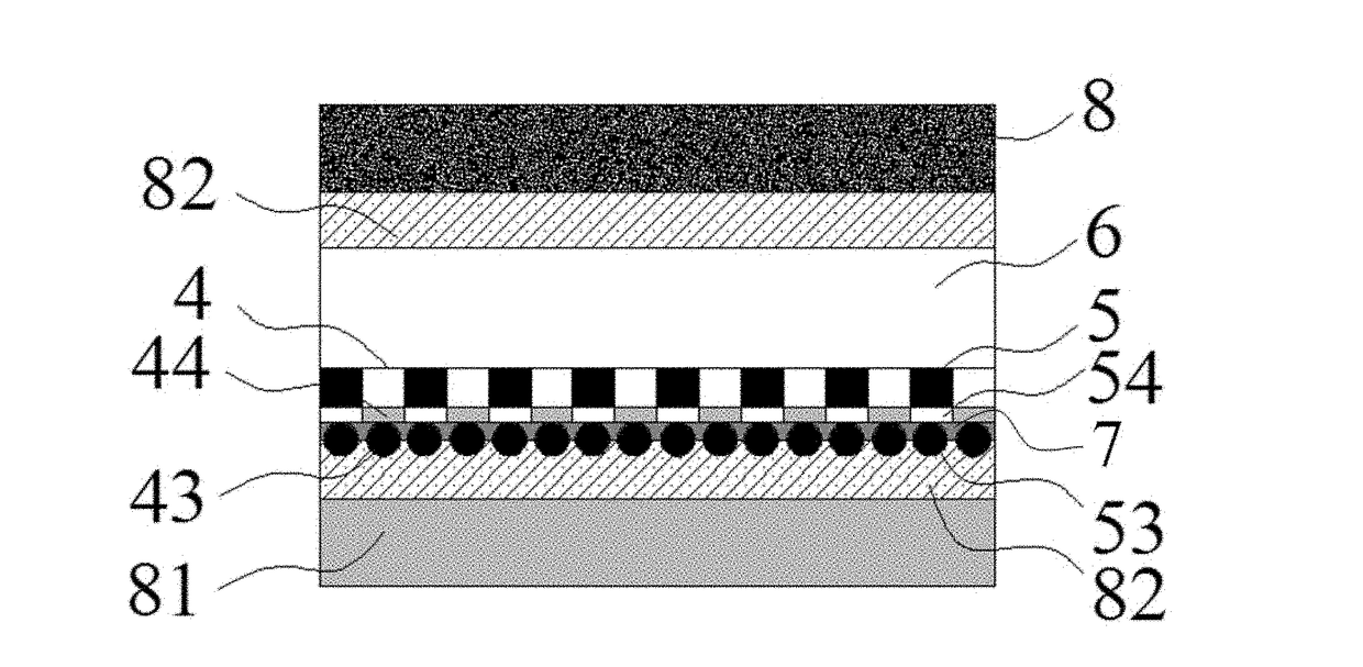
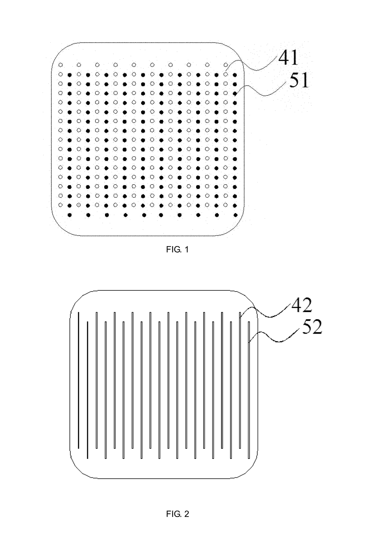
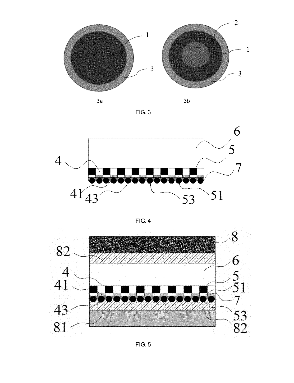
[0069]As shown in FIG. 1 and FIG. 4, a main-gate-free and high-efficiency back-contact solar cell module comprises cells and an electrical connection layer. The cell comprises a N-type monocrystal silicon substrate 6, the back side of which has P-electrodes connected to a P-type doping layer 5 and N-electrodes connected to a N-type doping layer 4, with a thermoplastic resin or thermosetting resin being provided at an insulating layer 7 between the P-electrodes and the N-electrodes. Wherein, the P-electrodes are dotted P-electrodes 51, and the N-electrodes are dotted N-electrodes 41; the dotted P-electrodes 51 and the dotted N-electrodes 41 are arranged alternately; and there are total 2080 dotted P-electrodes 51 and dotted N-electrodes 41. The diameter of the dotted P-electrodes 51 is 0.8 mm, and the distance between two adjacent dotted P-electrodes 51 is 1.5 mm. The diameter of the dotted N-electrodes 41 is 0.7 mm, the distance between two adjacent dotted N-electrodes 41 is 1.5 mm,...

embodiment 2

[0082]As shown in FIG. 1 and FIG. 4, a main-gate-free and high-efficiency back-contact solar cell module comprises cells and an electrical connection layer. The cell comprises a N-type monocrystal silicon substrate 6, the back side of which has P-electrodes connected to a P-type doping layer 5 and N-electrodes connected to a N-type doping layer 4, with a thermoplastic resin or thermosetting resin being provided at an insulating layer 7 between the P-electrodes and the N-electrodes. As shown in FIG. 1, the P-electrodes are dotted P-electrodes 51, and the N-electrodes are dotted N-electrode 41; the dotted P-electrodes 51 and the dotted N-electrodes 41 are arranged alternately; and the total number of dotted P-electrodes 51 and dotted N-electrodes 41 is 24200. The diameter of the dotted P-electrodes 51 is 0.5 mm, and the distance between two adjacent dotted P-electrodes 51 is 1.4 mm. The diameter of the dotted N-electrodes 41 is 0.4 mm, the distance between two adjacent dotted N-electr...

embodiment 3

[0095]As shown in FIG. 2 and FIG. 4, a main-gate-free and high-efficiency back-contact solar cell module comprises cells and an electrical connection layer. The cell comprises a N-type monocrystal silicon substrate 6, the back side of which has a P-type doping layer 5 and a N-type doping layer 4, with linear P-electrode regions 52 are formed on the P-type doping layer 5, linear N-electrode regions 42 are formed on the N-type doping layer 4, and the linear P-electrode regions 52 and the linear N-electrode regions 42 are alternately arranged. The width of the linear P-electrode regions 52 is 0.7 mm, and the distance between adjacent linear P-electrode regions 52 is 1.5 mm. The width of the linear N-electrode regions 42 is 0.5 mm, the distance between adjacent linear N-electrode regions 42 is 1.5 mm, and the center distance between the linear P-electrode regions 52 and the linear N-electrode regions 42 is 2.0 mm. The conversion efficiency of the cell is 20.5%. An insulating layer 7 is ...


PUM


Abstract

The present invention relates to the field of solar cells, and in particular to a main-gate-free and high-efficiency back-contact solar cell module, a main-gate-free and high-efficiency back-contact solar cell assembly, and a preparation process thereof. The solar cell module, comprising cells and an electrical connection layer, a backlight side of the cells having P-electrodes connected to a P-type doping layer and N-electrodes connected to a N-type doping layer, is characterized in that the electrical connection layer comprises a number of parallel leads each electrically connected to the P-electrodes or the N-electrodes. The present invention has the beneficial effect that a main-gate-free and high-efficiency back-contact solar cell module, a main-gate-free and high-efficiency back-contact solar cell assembly, and a preparation process thereof are provided, which can effectively the short-circuiting of the P-electrodes and the N-electrodes and has the advantages of low cost, high hidden-cracking resistance, high efficiency and high stability.

Description

TECHNICAL FIELD[0001]The present invention relates to the field of solar cells, and in particular to a main-gate-free and high-efficiency back-contact solar cell module, a main-gate-free and high-efficiency back-contact solar cell assembly, and a preparation process thereof.BACKGROUND OF THE PRESENT INVENTION[0002]Energy is the material basis of human activities. With the continuous development and progress of society, the demand for energy is increasing. The traditional fossil energy, belonging to non-renewable energy, has been difficult to meet the demands of the social development. Therefore, in recent years, new energy and renewable energy have been widely researched and utilized in countries all over the world. Among others, the solar power generation technology has attracted much attention due to its advantages of capability of converting sunlight into electric power, easy operation, environmental protection and no pollution, and high energy utilization. Solar power generation...

Claims


Application Information

Patent Timeline
Patent Type & Authority Applications(United States)
IPC IPC(8): H01L31/05H01L31/18H01L31/048H01L31/0216H01L31/0224H01L31/02
CPCH01L31/0516H01L31/022441H01L31/0201H01L31/1864H01L31/02167H01L31/1876H01L31/0481H01L31/18Y02E10/50H01L31/0512Y02P70/50H01L31/0504H01L31/06
Inventor LIN, JIANWEIXIA, WENJINSUN, YUHAIZHANG, YUZHENG
Owner JOLYWOOD SUZHOU SUNWATT
Why Eureka
Try Eureka