Method and structure of manufacturing a high-Q inductor with an air trench

a manufacturing method and high-q technology, applied in the direction of semiconductor devices, semiconductor/solid-state device details, inductances, etc., can solve the problems of not meeting desirable requirements, the quality factor of inductors manufactured by semiconductor technology is less than 5, and the application of certain circuits in specific areas is not completely developed. , to achieve the effect of reducing parasitic capacitance, reducing series resistance, and high quality factor

Inactive Publication Date: 2002-03-12
WINBOND ELECTRONICS CORP
View PDF6 Cites 42 Cited by
  • Summary
  • Abstract
  • Description
  • Claims
  • Application Information

AI Technical Summary

Benefits of technology

is to provide a method and a structure of manufacturing an inductor with a high quality factor and an air trench in a monolithic circuit. The inductor manufactured by the invention has a lower series resistance and a lower parasitic capacitance. Therefore, the inductor of the invention has lower energy losses, a higher quality factor and a higher operating frequency.
To attain the above-stated object, an inductor in a monolithic circuit according to the invention has the following structure. A plurality of spiral metal lines formed over a substrate. A plurality of dielectric layers, each of which is formed between two adjacent spiral metal lines. A plurality of via plugs formed in the dielectric layers to connect two adjacent spiral metal lines to each other. A spiral air trench formed along the spacing of the spiral metal lines in the dielectric layers. In such a structure having a plurality of spiral metal lines stacked on each other with the via plugs therebetween, the series resistance thereof is greatly decreased without widening the inductor. Moreover, air contained in the spiral air trench with a lower dielectric constant can efficiently reduce the parasitic capacitance of the inductor. Hence, the inductor manufactured based on the structure has a higher quality factor.

Problems solved by technology

However, miniaturization techniques have not been completely developed yet for certain circuits applied in specific areas, including, for example, radio frequency (RF) circuits, which are applied in communication equipment, such as cellular telephones (i.e., mobile telephones), cordless telephones, wireless modems and son on.
Currently, the quality factor of inductors manufactured by semiconductor technology is less than 5, which does not meet desirable requirements.
Although certain low-resistance metals, such as gold, can be used to increase the quality factor, it cannot be implemented by the current semiconductor technology.
However, this increases the area occupied by the metal line and the parasitic capacitance C.sub.d that follows.
The parasitic capacitance decreases the self-resonance frequency of the inductor, which, as a result, limits the range of the operating frequency thereof.

Method used


Image

  • Method and structure of manufacturing a high-Q inductor with an air trench
  • Method and structure of manufacturing a high-Q inductor with an air trench
  • Method and structure of manufacturing a high-Q inductor with an air trench

Examples


Embodiment Construction

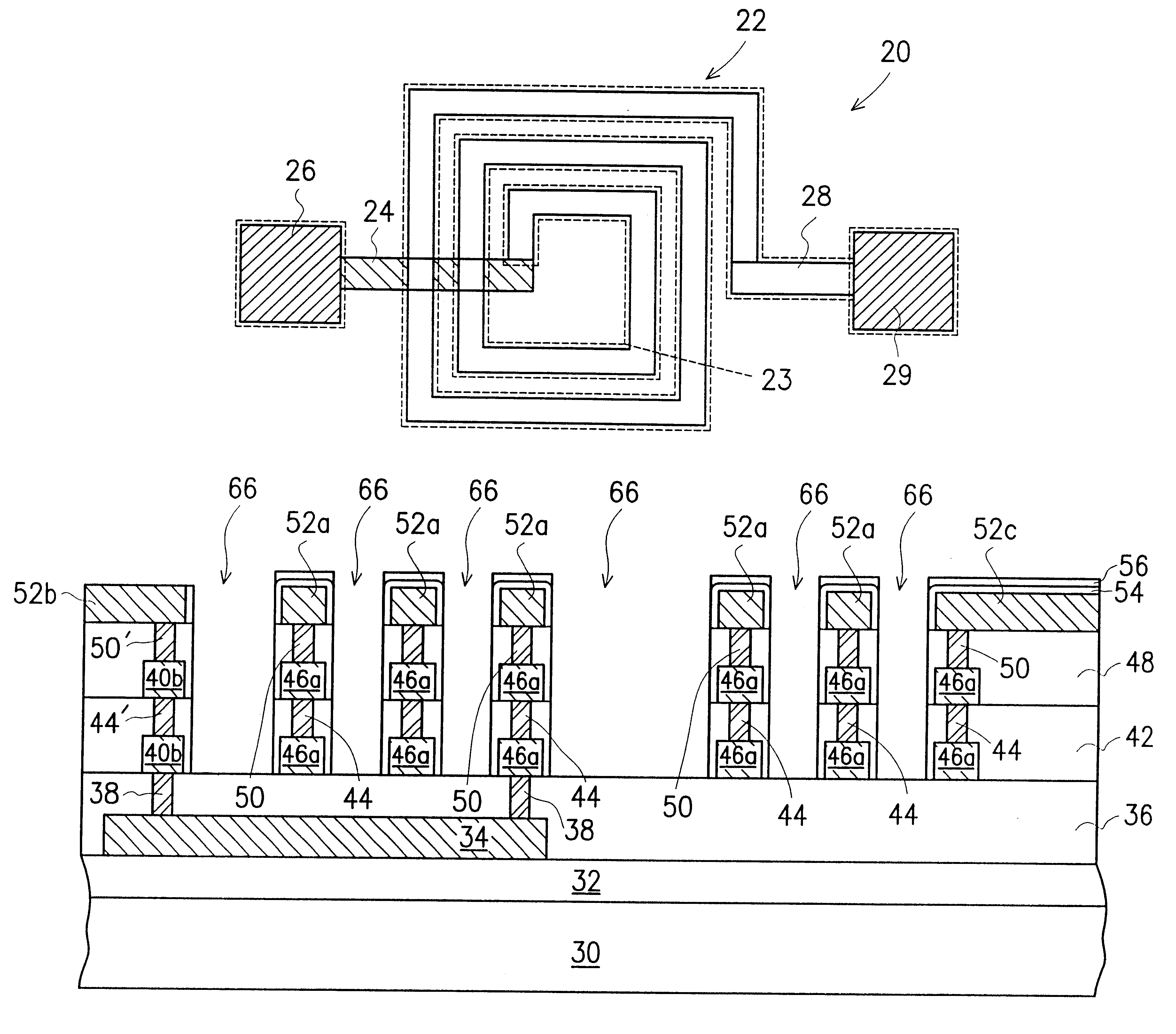
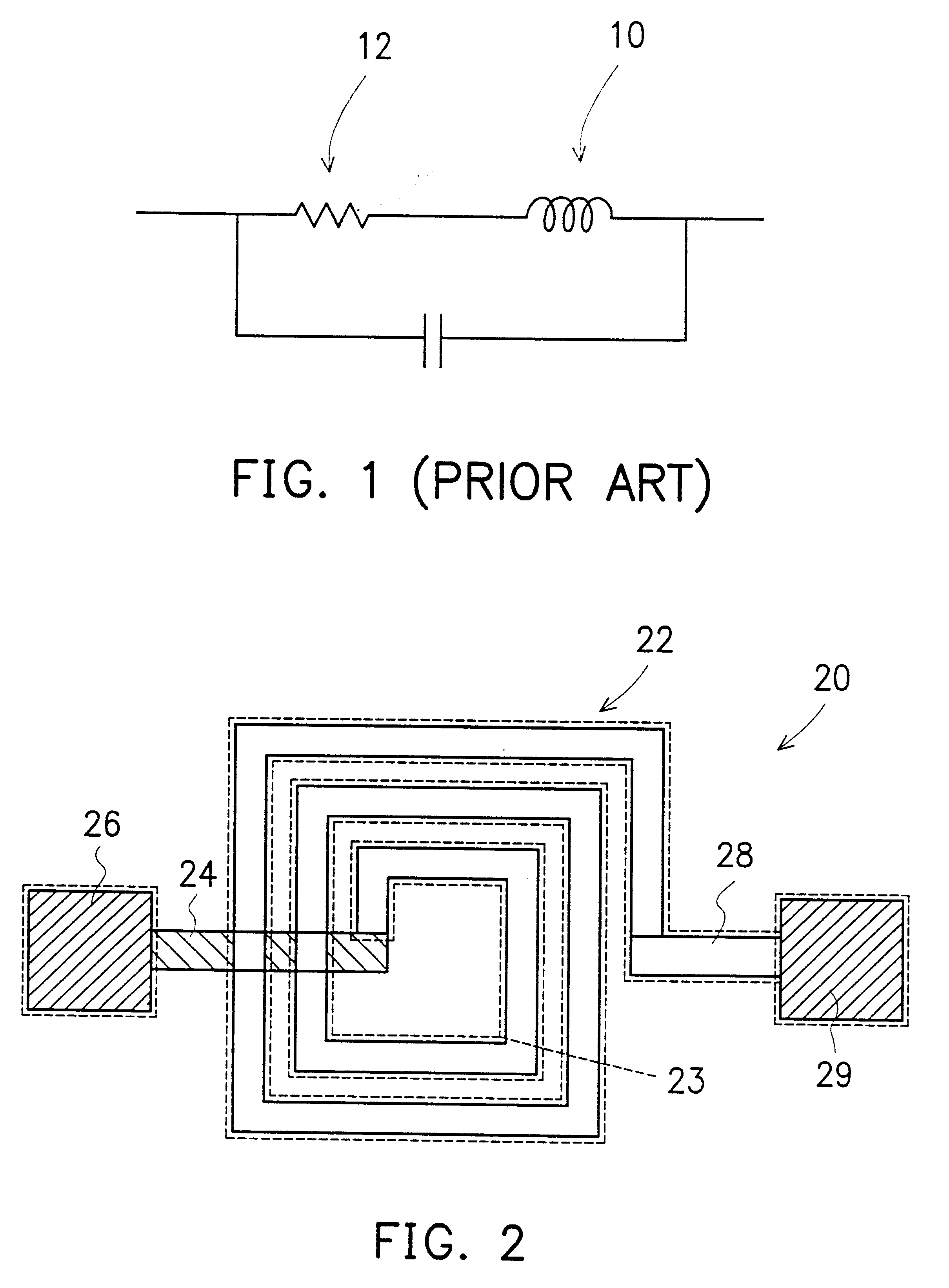
FIG. 2 is a top view of an inductor manufactured by a preferred embodiment of the invention. In FIG. 2, an inductor 20 formed on a semiconductor substrate includes a spiral conductive line 22. One end of the spiral conductive line 22 is electrically connected to a first bonding pad 26 via a first connective line 24 while the other end thereof is electrically connected to a second bonding pad 29 via a second connective line 28. The bonding pads 26 and 29 are used to electrically connect other circuits. A spiral air trench 23 (indicated by a dash line) is formed along the gap of the spiral conductive line 22 to reduce the parasitic capacitance thereof and increase the quality factor thereof.

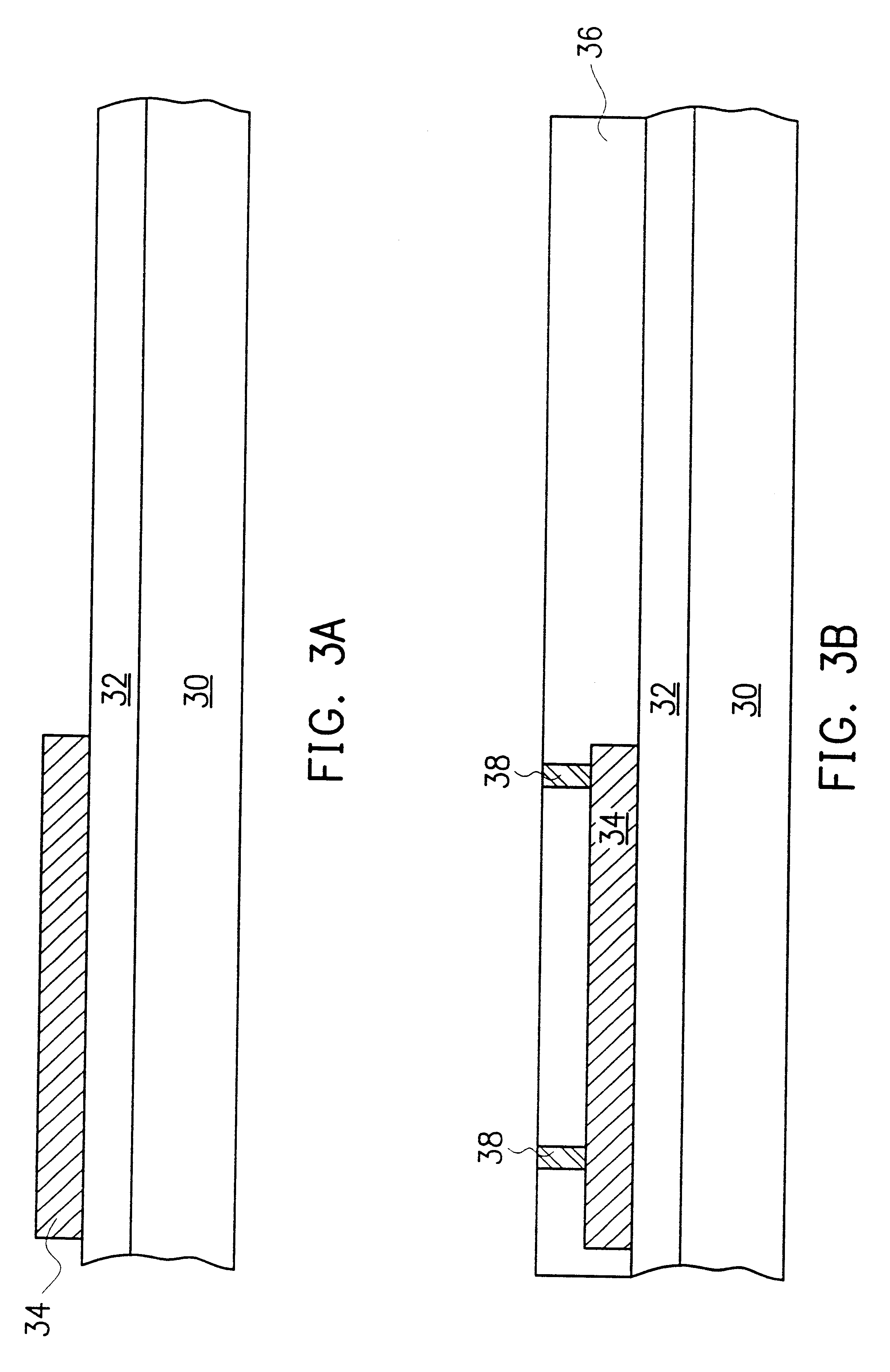
Referring to FIGS. 3A-3H, a method of manufacturing an inductor according to a preferred embodiment of the invention is shown. In FIG. 3A, a lower metal line 34, such as an aluminum line, is formed by sputtering and photolithography on an insulator 32, such as a silicon oxide layer, which is deposi...


PUM


Abstract

The structure of a high-Q inductor applied in a monolithic circuit according to the invention comprises a plurality of spiral metal lines and a plurality of dielectric layers, each dielectric layer formed between two adjacent spiral metal lines. Furthermore, via plugs are formed in each dielectric layer to electrically connect two adjacent spiral metal lines. A spiral air trench is formed along the spacing of the spiral metal lines in the dielectric layers. Therefore, the 3D-structure of the inductor of the invention can greatly reduce the series resistance thereof without widening the spiral metal lines. In addition, the spiral air trench, filled with air which has a lower dielectric constant, can efficiently reduce the parasitic capacitance between the spacing of the spiral metal lines. As a result, the inductor of the invention has a higher quality factor at a proper RF operating frequency region.

Description

1. Field of the InventionThe invention relates to a method and a structure of manufacturing an inductor in a monolithic circuit, and more particularly to a method and a structure of manufacturing an inductor with a high-quality factor and an air trench.2. Description of the Related ArtThe continuous miniaturization of integrated circuits (ICs) is a main trend in the semiconductor industry for the purpose of not only obtaining smaller sizes and lighter weights but also reducing manufacturing costs. Today, many digital circuits and analog circuits, such as complicated microprocessors and operational amplifiers, have been successfully mass produced into ICs by very large scale integrated (VLSI) technology. In general, the above-mentioned circuits include active devices, such as bipolar junction transistors (BJTs), field effect transistors (FETs) and diodes, and passive devices, such as resistors and capacitors.However, miniaturization techniques have not been completely developed yet f...

Claims


Application Information

Patent Timeline
Patent Type & Authority Patents(United States)
IPC IPC(8): H01L21/02H01L23/52H01L21/70H01L21/764H01L23/522H01L27/08
CPCH01L21/764H01L23/5227H01L27/08H01L28/10H01F2017/0046H01L2924/0002H01L2924/00
Inventor LIOU, PING
Owner WINBOND ELECTRONICS CORP
Why Eureka
Try Eureka