Method to fabricate a chip for the detection of biological elements

a technology of biological elements and fabrication methods, applied in the direction of material analysis, measurement devices, instruments by electric/magnetic means, etc., can solve the problems of insufficient detection sensitivity of electric detection devices, inability to precisely distribute channels, and inability to accurately detect the presence of biological elements

Active Publication Date: 2011-04-19
COMMISSARIAT A LENERGIE ATOMIQUE ET AUX ENERGIES ALTERNATIVES
View PDF4 Cites 3 Cited by
  • Summary
  • Abstract
  • Description
  • Claims
  • Application Information

AI Technical Summary

Benefits of technology

[0030]The biological receptors bonded at step c) may optionally be arranged in an encapsulating layer. This allows the stability of molecule binding to be improved, and allows use of a device with a large quantity of receptors.
[0038]This makes it possible to form blocks in said given material whose dimensions are greater than those of the gates, and thereby to overcome any alignment difficulties when it is subsequently desired to perform at least partial removal of the gates.

Problems solved by technology

The electric detection sensitivity of said device is insufficient.
This method does not allow precise distribution of the channels.
Also, with said method, the nanowires obtained have a length and diameter which are difficult to control, which creates dispersion between the electric characteristics of the different channels.
The fabrication of transistors to detect said circuit is difficult to implement.

Method used


Image

  • Method to fabricate a chip for the detection of biological elements
  • Method to fabricate a chip for the detection of biological elements
  • Method to fabricate a chip for the detection of biological elements

Examples


Embodiment Construction

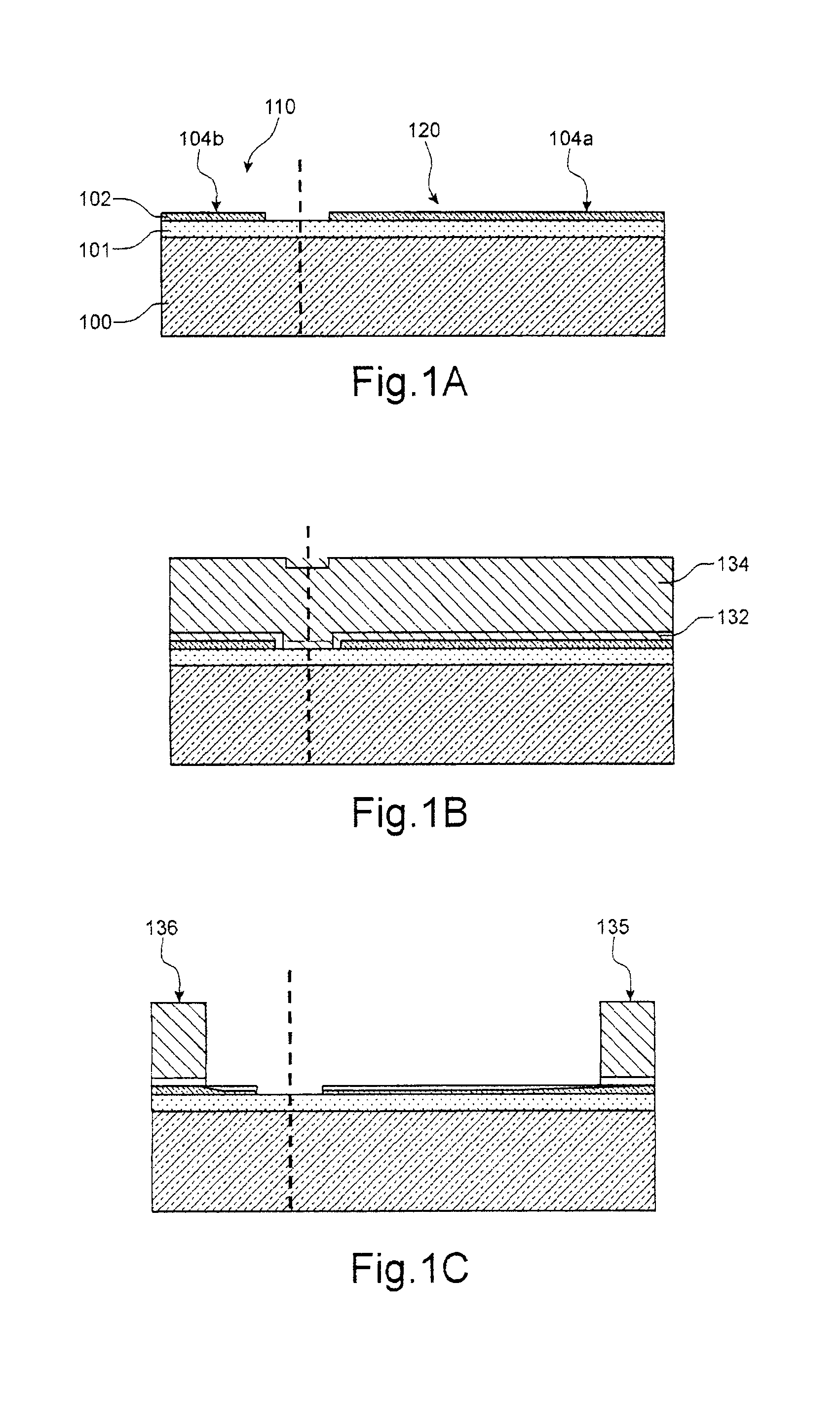
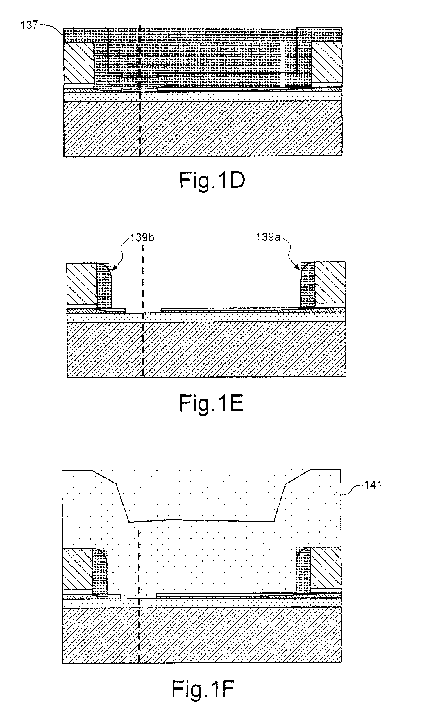
[0017]The present invention concerns a method to fabricate a microelectronic device provided with at least one circuit for the detection of biological elements, comprising the steps of:

[0018]a) fabricating, on a substrate, a plurality of transistors each comprising at least one gate formed of at least one layer containing at least one gate material on at least one layer of gate dielectric, said gate resting on a channel region,

[0019]b) removing, at least in part, the respective gate from one or more so-called “first-type transistors” from among said transistors, whilst the respective gate of one or more other so-called “second-type transistors” amongst said transistors, is protected,

[0020]c) binding or grafting biological receptors on a surface (S) of said first-type transistors, the surface facing their channel region.

[0021]The biological receptors, also called biological probes, can for example be in the form of DNA, oligo-nucleotides, proteins, enzymes, or antibodies.

[0022]Bindin...


PUM


Abstract

Improved method to fabricate a microelectronic device provided with at least one circuit to detect biological elements, comprising the steps of:a) forming transistors,depositing at least one layer in at least one insulating material (141) coating said transistors,forming one or more holes (143) in said layer of insulating material (141), so as to expose the upper face of the respective gate (135) of first-type transistors,filling the holes with a gate material,b) removing, at least in part, the respective gate (135) of the first-type transistors, whilst the gate of second-type transistors is protected, the method prior to or at the same time as said removal conducted at step b) further comprising the removal of said gate material.

Description

TECHNICAL AREA[0001]The invention relates to the field of microelectronics and more particularly to the field of microelectronic devices comprising at least one circuit for the detection of biological elements.[0002]The invention provides for and allows the co-integration, on one same substrate, of transistors dedicated to detecting biological elements such as biological markers, together with conventional transistors provided with a gate.[0003]It notably concerns a method to fabricate at least one microelectronic device comprising, on one same substrate, at least one circuit to detect biological elements and one or more other circuits for processing measurements.[0004]The invention also concerns the fabrication of an electronic chip allowing the automatic determination of a medical pre-diagnosis or medical diagnosis.STATE OF THE PRIOR ART[0005]The fabrication of devices to detect biological molecules on a chip is known.[0006]Document EP 1 557 884 A2 describes a biological detection...

Claims


Application Information

Patent Timeline
Patent Type & Authority Patents(United States)
IPC IPC(8): H01L21/336
CPCG01N27/4145
Inventor BUCKLEY, JULIENBILLOINT, OLIVIERDELAPIERRE, GUILLAUME
Owner COMMISSARIAT A LENERGIE ATOMIQUE ET AUX ENERGIES ALTERNATIVES
Why Eureka
Try Eureka