Bias circuit for a MOS device

a bias circuit and mos technology, applied in the field of bias circuits, can solve the problems of affecting the performance of the circuit, reducing the performance of many cmos circuits, and excessive power dissipation, so as to reduce the overall variation, improve the optimization of the circuit, and effectively adjust the threshold voltage

Inactive Publication Date: 2011-05-03
GLOBALFOUNDRIES INC
View PDF11 Cites 8 Cited by
  • Summary
  • Abstract
  • Description
  • Claims
  • Application Information

AI Technical Summary

Benefits of technology

[0008]Accordingly, a circuit is provided for controlling the body bias to the MOS devices to effectively adjust the threshold voltage and compensate for variation in process, temperature, and voltage. While this circuit will not eliminate all variation due to process, temperature, and voltage, it can significantly reduce the overall variation and allow for better optimization of circuit performance over corner conditions. This bias circuit can be used in a variety of applications, such as level-shifters, VCOs, phase rotators, etc.

Problems solved by technology

It is known that running these circuits at low supply voltages affect the performance of the circuits over process, temperatures and supply voltage variations.
However, the performance of many CMOS circuits degrades rapidly as the supply voltage approaches the sum of the threshold voltages of the NMOS and PMOS devices.
Organizing circuit performance for the low-voltage, low-temperature (high-Vt) corner typically results in excessive power dissipation at the high voltage, high-temperature (low-Vt) corner.

Method used


Image

  • Bias circuit for a MOS device
  • Bias circuit for a MOS device
  • Bias circuit for a MOS device

Examples


second embodiment

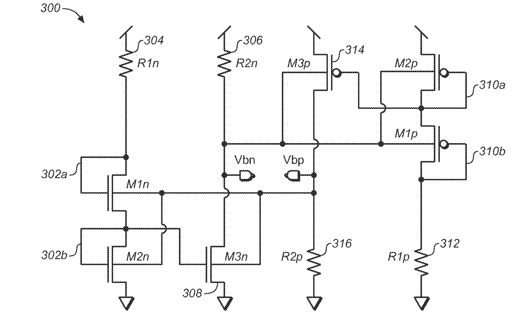
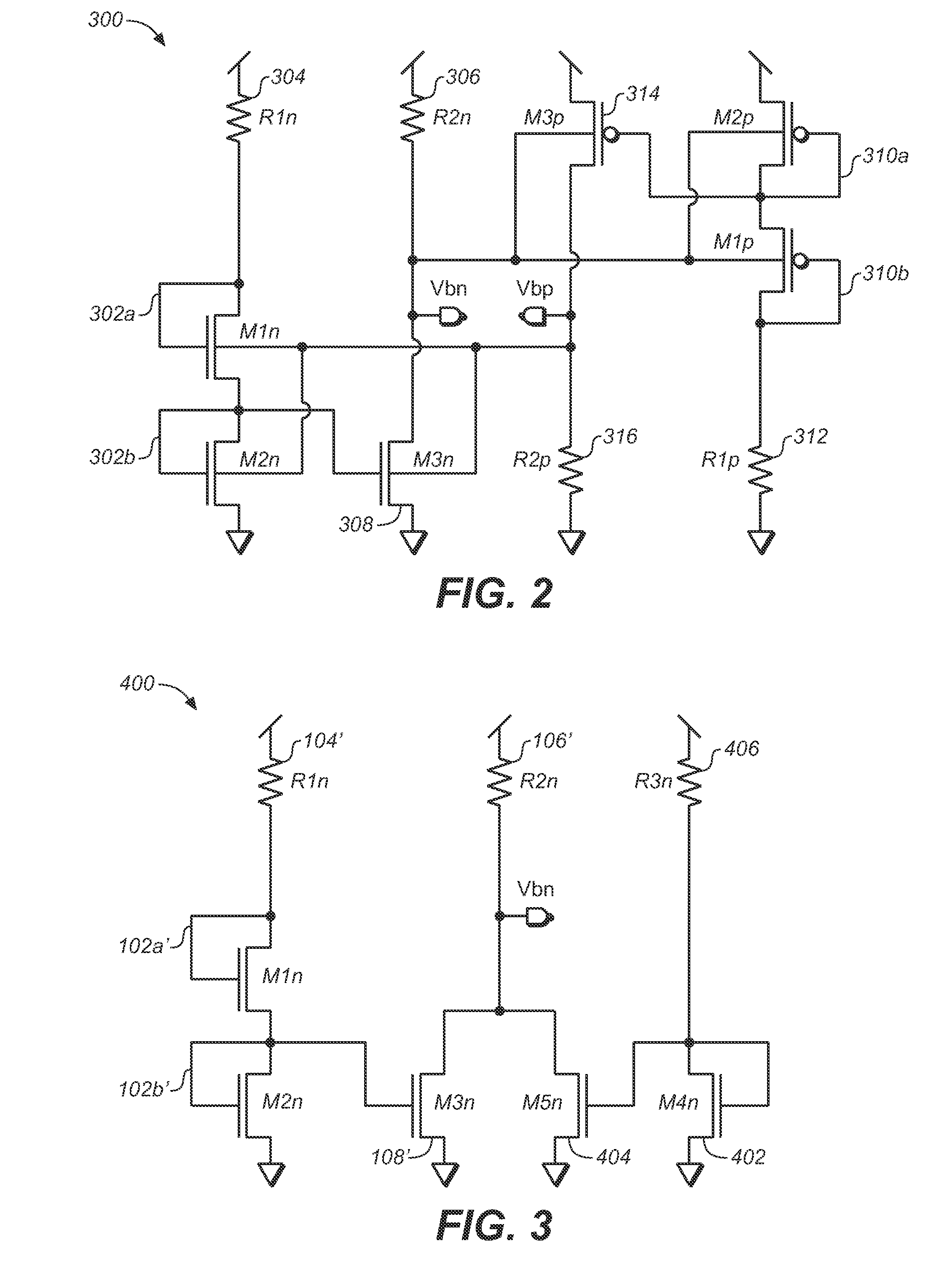
[0022]FIG. 2 is a bias circuit 300 in which the generated bias is being used in the circuit itself to bias the body of both NMOS and PMOS devices. In this embodiment, resistor 304 is coupled to diode connected transistors 302a and 302b, which are in turn, coupled to diode connected transistors 308 and resistor 306. Diode connected transistor 308 is coupled to resistor 316, which is coupled to ground. Resistor 306 is coupled to diode connected transistor 314, which is then coupled to transistor 310a and 310b. Transistors 310a and 310b are coupled to resistor 312, which is coupled to ground.

[0023]In this embodiment, the bias voltage, Vbp, is applied to the NMOS devices and the bias voltage, Vbn, is applied to the PMOS devices. Instead of compensating for pressure, voltage and temperature variations, the bias voltage increases the sensitivity to process, voltage and temperature variations and extends the range of the bias outputs, Vbp and Vbn, which may be beneficial in certain applica...

third embodiment

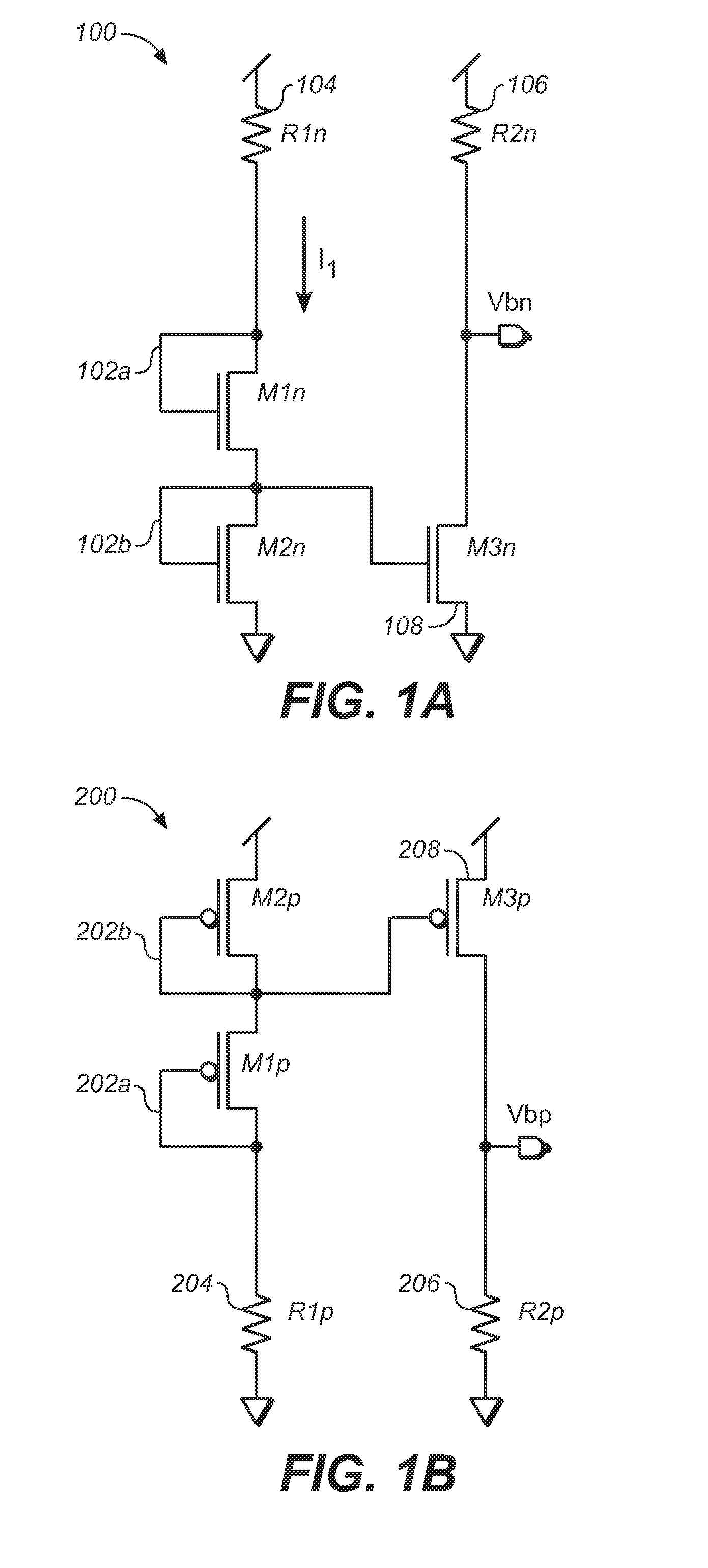
[0024]Finally, bias voltages with an arbitrary sensitivity to process, voltage and temperature variations can be generated by combining the outputs of multiple versions of the basic circuit. One such example is shown in FIG. 3. FIG. 3 is a schematic of only the NMOS portion of a substrate bias circuit 400. The left half of the circuit replicates that in FIG. 1. The right half is similar but contains a single diode-connected MOS device 402. MOS device 402 is connected to the diode connected transistor 402 which is then connected to resistor 406 and to ground. The MOS diode connected device 402 will have less temperature sensitivity than the stacked diodes 102a′ and 102b′. By adjusting the resistor values 104′, 106′ and 406 and the relative weights of current mirrors 108′ and 404′, an arbitrary sensitivity can be optimized between the two extremes. A complementary PMOS version can also be constructed utilizing PMOS devices.

[0025]Accordingly, by using a bias circuit in accordance with ...


PUM


Abstract

A method and circuit for providing a bias voltage to a MOS device is disclosed. The method and circuit comprise utilizing at least one diode connected circuit to provide a voltage that tracks process, voltage and temperature variations of a semiconductor device. The method and circuit includes utilizing a current mirror circuit coupled to the at least one diode connected circuit to generate a bias voltage for the body of the semiconductor device from the voltage. The bias voltage allows for compensation for the process, voltage and temperature variations.

Description

FIELD OF THE INVENTION[0001]The present invention relates generally to a semiconductor circuits and more particularly to bias circuits for low voltage applications.BACKGROUND OF THE INVENTION[0002]MOS circuits, particularly CMOS circuits, are utilized in a variety of applications. For example, these circuits are utilized in level shifters, oscillators, phase rotators, inverters, and the like. It is known that running these circuits at low supply voltages affect the performance of the circuits over process, temperatures and supply voltage variations.[0003]The power dissipation of CMOS circuits is roughly proportional to the square of the supply voltage, and so running these circuits at low supply voltages is important to achieve low power dissipation. However, the performance of many CMOS circuits degrades rapidly as the supply voltage approaches the sum of the threshold voltages of the NMOS and PMOS devices. The threshold voltage of the MOS devices is also a strong function of tempe...

Claims


Application Information

Patent Timeline
Patent Type & Authority Patents(United States)
IPC IPC(8): G05F3/02
CPCG05F3/205
Inventor CLEMENTS, STEVEN MARKCRANFORD, JR., HAYDEN C.DWARKA, AMAR CHANDRA MAHADEOEWEN, JOHN FARLEY
Owner GLOBALFOUNDRIES INC
Why Eureka
Try Eureka