Optical waveguide device with an adiabatically-varying width

a waveguide and optical waveguide technology, applied in the field of optical waveguide devices, can solve the problems of propagation loss of light in these devices, limit the utility of the resonator for many applications, and propagation loss can also occur

Active Publication Date: 2011-05-10
NAT TECH & ENG SOLUTIONS OF SANDIA LLC
View PDF3 Cites 73 Cited by
  • Summary
  • Abstract
  • Description
  • Claims
  • Application Information

AI Technical Summary

Benefits of technology

[0010]The present invention relates to an optical waveguide apparatus which comprises an optical waveguide having a waveguide bend therein, with the waveguide bend having a width which adiabatically varies with distance between a minimum value of the width proximate to a pair of opposite ends of the waveguide bend and a maximum value of the width proximate to a midpoint of the waveguide bend; and at least one connecting member attached to the waveguide proximate to the midpoint of the waveguide bend. An impurity-doped region can be formed within the optical waveguide at a location proximate to the maximum value of the width of the waveguide bend to change an effective index of refraction within the waveguide bend in response to a voltage applied to the impurity-doped region. The optical waveguide can be used to form an optical delay line. Another optical waveguide can be provided in the apparatus to form an interferometer (e.g. a Mach-Zehnder interferometer) with the impurity-doped region providing a variable phase delay in the interferometer to provide for a modulation or switching of light.

Problems solved by technology

Such contacts, however, can perturb the resonant modes of light being transmitted in the optical waveguide devices; and this can result in propagation losses of the light in these devices.
In a microring resonator, the reduction of a quality factor, Q, in the microring resonator will limit the utility of the resonator for many applications including communications where a large resonator Q is needed for narrowband filtering, switching, or modulation.
In other types of optical waveguide devices including interferometers, phase shifters and delay lines, propagation losses can also occur from electrically contacting an optical waveguide therein.

Method used


Image

  • Optical waveguide device with an adiabatically-varying width
  • Optical waveguide device with an adiabatically-varying width
  • Optical waveguide device with an adiabatically-varying width

Examples


Embodiment Construction

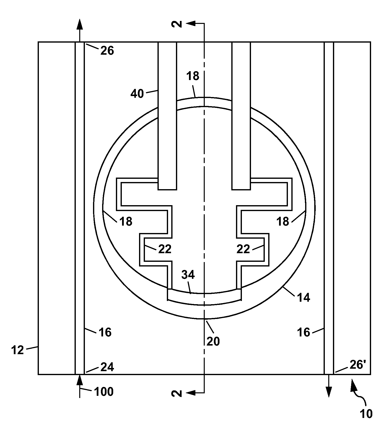
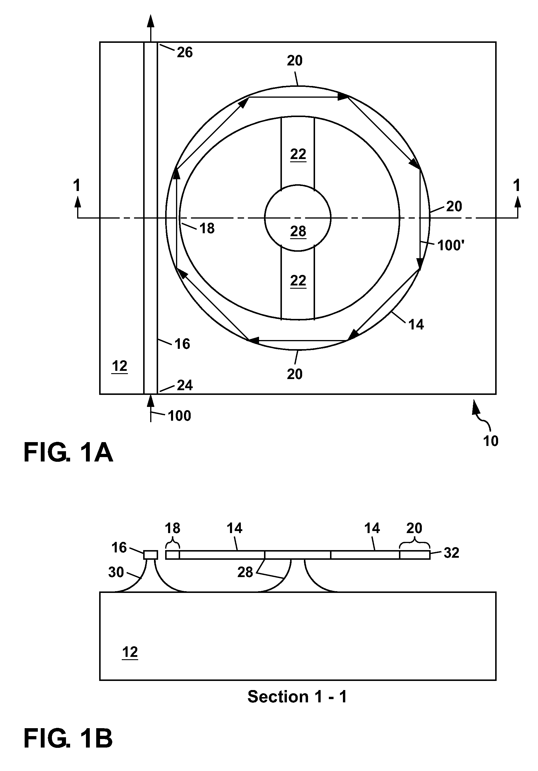
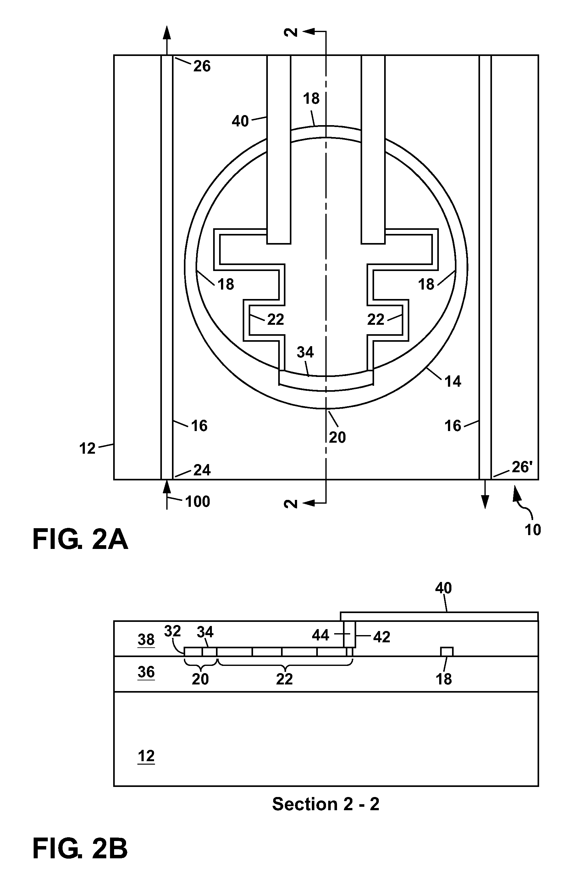
[0037]The optical waveguide devices of the present invention can be formed as either optical ring resonators or optical waveguides having a waveguide bend therein. A series of examples of optical ring resonators will first be presented to illustrate the present invention. This will be followed by a series of examples of optical waveguide devices which do not include an optical ring resonator with a closed-loop optical path, but which instead utilize a curved portion of an open-loop optical waveguide which is referred to herein as a waveguide bend (also termed a microbend).

[0038]Referring to FIG. 1, there is shown a first example of an optical waveguide apparatus 10 according to the present invention. This device 10 comprises a substrate 12 on which an optical waveguide ring 14 (also referred to herein as an optical ring resonator or simply as a ring resonator) is supported. An optical waveguide 16 is also provided on the substrate 12 to evanescently couple light between the optical ...


PUM

PropertyMeasurementUnit
sizeaaaaaaaaaa
outer radiusaaaaaaaaaa
widthaaaaaaaaaa

Abstract

Optical waveguide devices are disclosed which utilize an optical waveguide having a waveguide bend therein with a width that varies adiabatically between a minimum value and a maximum value of the width. One or more connecting members can be attached to the waveguide bend near the maximum value of the width thereof to support the waveguide bend or to supply electrical power to an impurity-doped region located within the waveguide bend near the maximum value of the width. The impurity-doped region can form an electrical heater or a semiconductor junction which can be activated with a voltage to provide a variable optical path length in the optical waveguide. The optical waveguide devices can be used to form a tunable interferometer (e.g. a Mach-Zehnder interferometer) which can be used for optical modulation or switching. The optical waveguide devices can also be used to form an optical delay line.

Description

CROSS REFERENCE TO RELATED APPLICATIONS[0001]This is a continuation-in-part of application Ser. No. 12 / 100,004, filed Apr. 9, 2008 now U.S. Pat. No. 7,616,850.GOVERNMENT RIGHTS[0002]This invention was made with Government support under Contract No. DE-AC04-94AL85000 awarded by the U.S. Department of Energy. The Government has certain rights in the invention.FIELD OF THE INVENTION[0003]The present invention relates in general to photonic integrated circuits, and in particular to optical waveguide devices containing a waveguide bend or a ring resonator which has an adiabatically-varying width to allow for a mechanical or an electrical connection to be made without substantially perturbing the transmission of light therein. The optical waveguide devices of the present invention can be used, for example, to form interferometers, phase shifters, delay lines, filters, modulators and switches.BACKGROUND OF THE INVENTION[0004]Optical waveguide devices can be used as optical phase shifters a...

Claims


Application Information

Patent Timeline
Patent Type & Authority Patents(United States)
IPC IPC(8): G02F1/035G02B6/26
CPCB82Y20/00G02B6/1223G02B6/1228G02B6/125G02B6/29335G02F1/225G02B6/12007G02F2203/20G02B2006/12061G02B2006/12142G02B2006/12145G02F1/0147G02F1/2257G02F1/3132G02F2001/0151G02F2001/212G02F2201/063G02F2202/06G02F2202/104G02F2202/105G02F2203/15G02F1/0151G02F1/212
Inventor WATTS, MICHAEL R.NIELSON, GREGORY N.
Owner NAT TECH & ENG SOLUTIONS OF SANDIA LLC
Why Eureka
Try Eureka