
Signal detecting circuit

a signal detection and circuit technology, applied in pulse manipulation, pulse technique, instruments, etc., can solve the problems of increasing manufacturing steps, increasing costs, and inability to accurately detect the received signal, and achieve the effect of accurately detecting presence and absen

Active Publication Date: 2011-05-17
RENESAS ELECTRONICS CORP
View PDF5 Cites 9 Cited by
  • Summary
  • Abstract
  • Description
  • Claims
  • Application Information

AI Technical Summary

Benefits of technology

[0017]An object of the invention is to provide a signal detecting circuit that can accurately detect presence and absence of a differential signal of a minute amplitude.
[0018]Another object of the invention is to provide a signal detecting circuit that allows flexible setting of a criterion for determining a no-signal state, and can accurately detect the no-signal state.
[0023]The differential signal is received with a high impedance, and the complementary signal line pair has no current flowing path. Therefore, such a situation can be avoided that both center potentials of the paired complementary signal lines transmitting the differential signal rise toward a high-side power supply voltage level. Thus, the presence of the received signal can be detected.
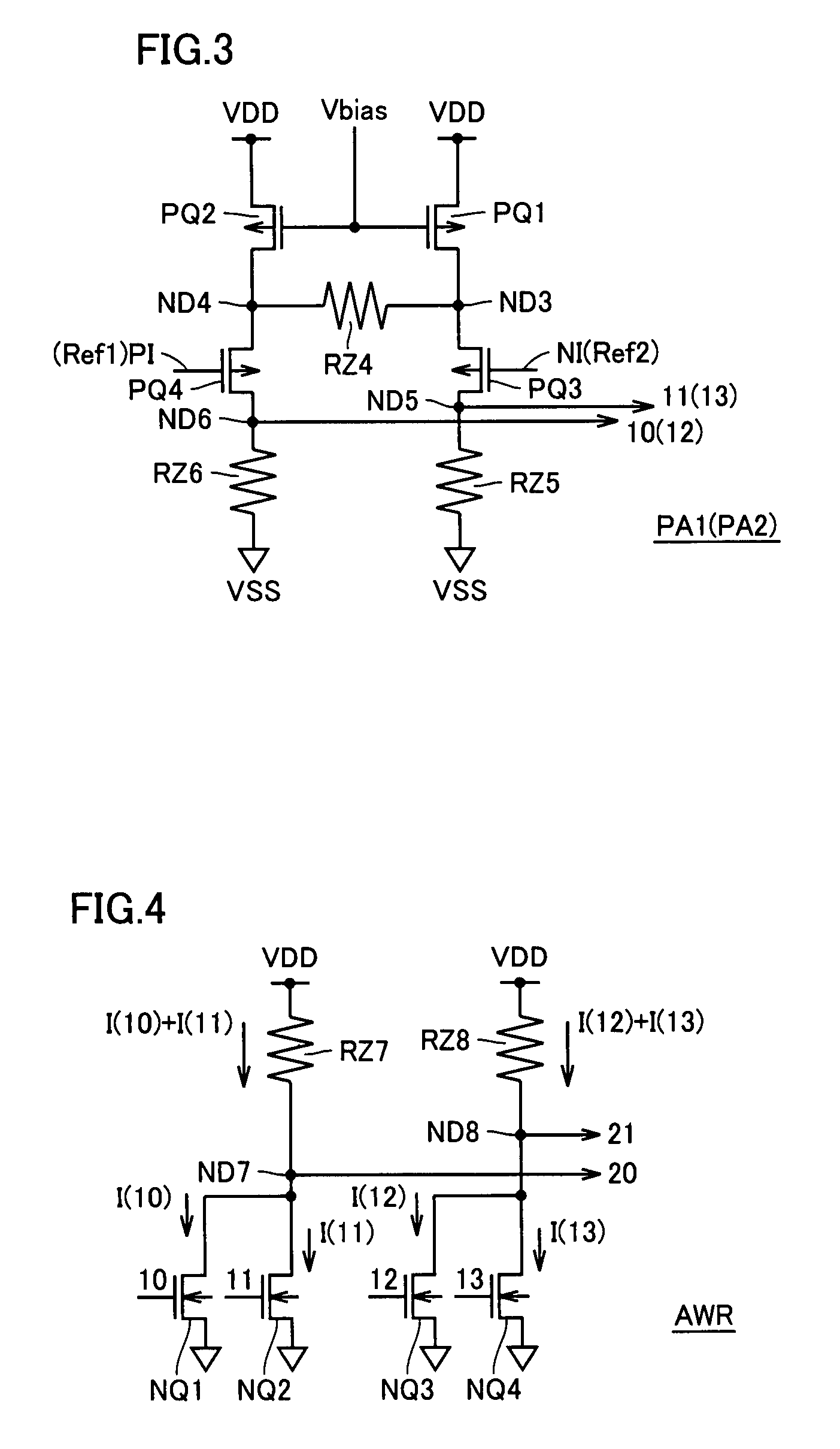
[0024]The detection is made based on the comparison with the reference voltages, using the transistor pair, and the accurate detection can be performed even when the differential signal amplitude is small. Further, it is not required to reduce threshold voltages of the transistor pair, and increase in number of manufacturing steps can be suppressed.

Problems solved by technology

Therefore, the MOS transistors for the reception detection must be made different in threshold voltages from MOS transistors of other circuitry, so that a problem of increase of manufacturing steps and therefore increase of cost arise.
This current supplied from the second MOS transistor acts to reduce the amplitude (the minute amplitude) of the differential signal, and it may be impossible to detect accurately the received signal.
This state causes a problem that the received signal can no longer be detected accurately.
Further, when a failure in data transmission path for transmission and reception is to be detected through the no-signal state, a criterion for such failure detection cannot be set flexibly depending on a use environment.

Method used


Image

  • Signal detecting circuit
  • Signal detecting circuit
  • Signal detecting circuit

Examples


first embodiment

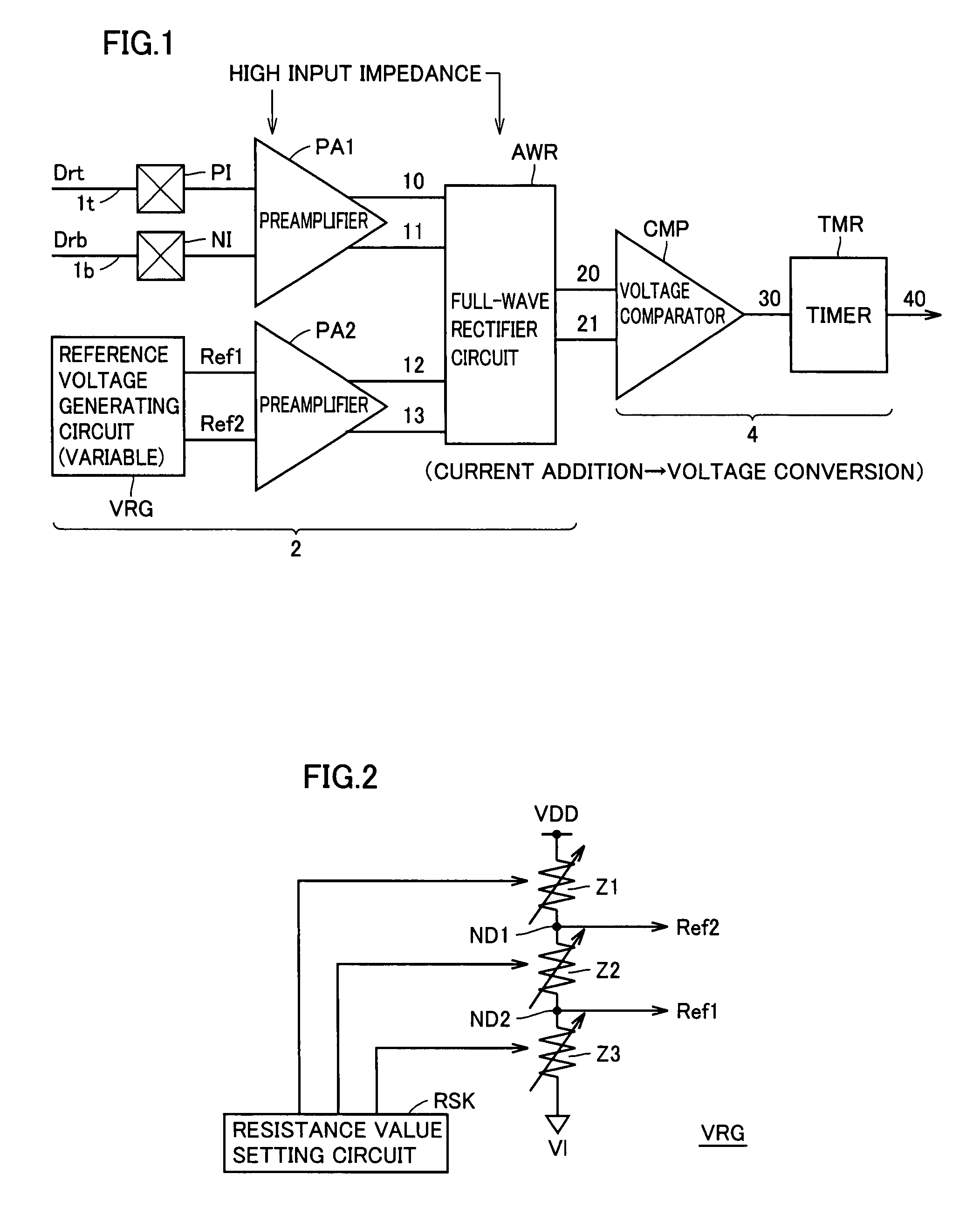
[0044]FIG. 1 schematically shows a whole construction of a signal detecting circuit according to a first embodiment of the invention. In FIG. 1, the signal detecting circuit includes an input circuit 2 produces, according to a difference value of a differential signal formed of complementary signal Drt, Drb transmitted through complementary signals 1t and 1b and a difference value between reference voltages Ref1 and Ref2, signals 20 and 21 indicating magnitudes of these difference values, and an internal signal producing circuit 4 that produces a signal 40 indicating a logical level of differential signal Drt, Drb according to complementary output signals 20 and 21 of input circuit 2.

[0045]In signal transmission, differential signal Drt, Drb is formed of complementary signals that change toward higher and lower sides by substantially the same amplitude ΔV with a reference voltage (a common level) being a center. Accordingly, the amplitude of differential signal Drt, Drb is given by ...

second embodiment

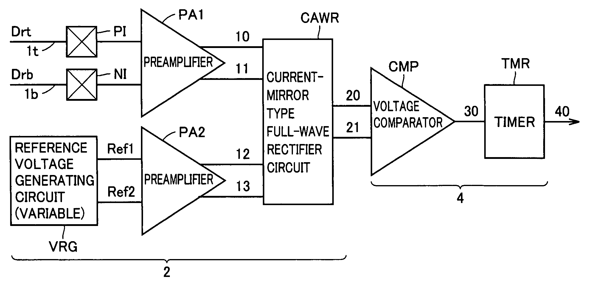
[0113]FIG. 10 schematically shows a whole construction of a signal detecting circuit according to a second embodiment of the invention. The signal detecting circuit shown in FIG. 10 differs from that in FIG. 1 in the following configurations. In input circuit 2, a current mirror type full-wave rectifier circuit CAWR is employed for full-wave rectifier circuit AWR. In the current mirror type full-wave rectifier circuit CAWR, differential amplification is performed by a current mirror operation according to the added value of output signals 10 and 11 of preamplifier PA1 and the added value of output signals 12 and 13 of preamplifier PA2, and complementary output signals 20 and 21 are produced.

[0114]Other configurations of the signal detecting circuit shown in FIG. 10 are the same as those of the signal detecting circuit shown in FIG. 1. The corresponding components are allotted the same reference numerals, and description thereof will not be repeated.

[0115]FIG. 11 shows an example of ...

third embodiment

[0136]FIG. 13 schematically shows a whole construction of a signal detecting circuit according to a third embodiment of the invention. The signal detecting circuit shown in FIG. 13 differs from the signal detecting circuit shown in FIG. 1 in the following configurations. In input circuit 2, the voltages V1 and V2 applied to preamplifier PA2 are at fixed voltage levels. The full-wave rectifier circuit receiving output signals 10-13 of preamplifiers PA1 and PA2 is formed of an output-amplitude-variable full-wave rectifier circuit VAWR. Output-amplitude-variable full-wave rectifier circuit VAWR adjusts the comparison reference amplitude, to adjust the detection threshold of the amplitude of differential signal Drt, Drb.

[0137]FIG. 14 shows an example of the construction of output-amplitude-variable full-wave rectifier circuit VAWR shown in FIG. 13. Output-amplitude-variable full-wave rectifier circuit VAWR shown in FIG. 14 differs from full-wave rectifier circuit AWR shown in FIG. 1 in ...


PUM


Abstract

A full-wave rectifier circuit receives complementary signals and produces a current corresponding to an added value of differential signals at different levels. A voltage comparator performs a comparison between output signals produced and subjected to current addition and voltage conversion by the full-wave rectifier circuit. A timer detects whether an output signal of the voltage comparator is kept in the same state for a predetermined time or more, and produces a signal indicating a result of the detection. A signal detecting circuit that can accurately identify a state of digital signals of a minute amplitude transferred through a pair of complementary signal lines is achieved without complicating manufacturing steps.

Description

BACKGROUND OF THE INVENTION[0001]1. Field of the Invention[0002]The present invention relates to a signal detecting circuit, and particularly to a signal detecting circuit for detecting a differential signal of a minute amplitude.[0003]2. Description of the Background Art[0004]In a data communications field, signals are transmitted at high speed. Differential signals of small amplitudes are used as transmission signals for fast transmission and low current consumption. The differential signal is formed of a pair of complementary signals, which are set to high and low levels relative to a reference potential, respectively. Such differential signal has a signal amplitude doubled as compared with the case of transferring a single signal, and therefore, the differential signal is usually used as the transmission signal in fast digital communications.[0005]In data transmission, synchronization of data must be established between transmission and reception sides. A clock signal is used fo...

Claims


Application Information

Patent Timeline
Patent Type & Authority Patents(United States)
IPC IPC(8): H03K5/153
CPCH03F3/45179H03F3/45475H03F2203/45138H03F2200/78H03F2200/453
Inventor UCHIKI, HIDEKI
Owner RENESAS ELECTRONICS CORP
Learn More