Optical element unit

a technology of optical elements and units, applied in the field of optical element units, can solve the problems of considerable effort, adverse effects on imaging accuracy, and on the overall quality of exposure process, and achieve good and long-term reliable imaging properties

Active Publication Date: 2011-05-17
CARL ZEISS SMT GMBH
View PDF6 Cites 4 Cited by
  • Summary
  • Abstract
  • Description
  • Claims
  • Application Information

AI Technical Summary

Benefits of technology

[0011]It is thus an object of the present invention to, at least to some extent, overcome the above disadvantages and to provide good and long term reliable imaging properties of an optical system used in an exposure process.
[0012]It is a further object of the present invention to maintain imaging accuracy of an optical system used in an exposure process by reducing the sensitivity of the optical system to pressure differences between an atmosphere within an optical element unit of the optical system and the environment surrounding the optical element unit.

Problems solved by technology

Depending on the design of the respective last lens element, in particular on the optical sensitivity of the last lens element to position variations, such position variations may have a considerable adverse effect on the imaging accuracy and, thus, on the overall quality of the exposure process.
To largely avoid these effects, currently, considerable effort is necessary to hold such an ultimate optical element in a manner which is as rigid as possible.
This is particularly complicated if, for other purposes, the ultimate optical element has to be held in an adjustable manner.

Method used


Image

  • Optical element unit
  • Optical element unit
  • Optical element unit

Examples


first embodiment

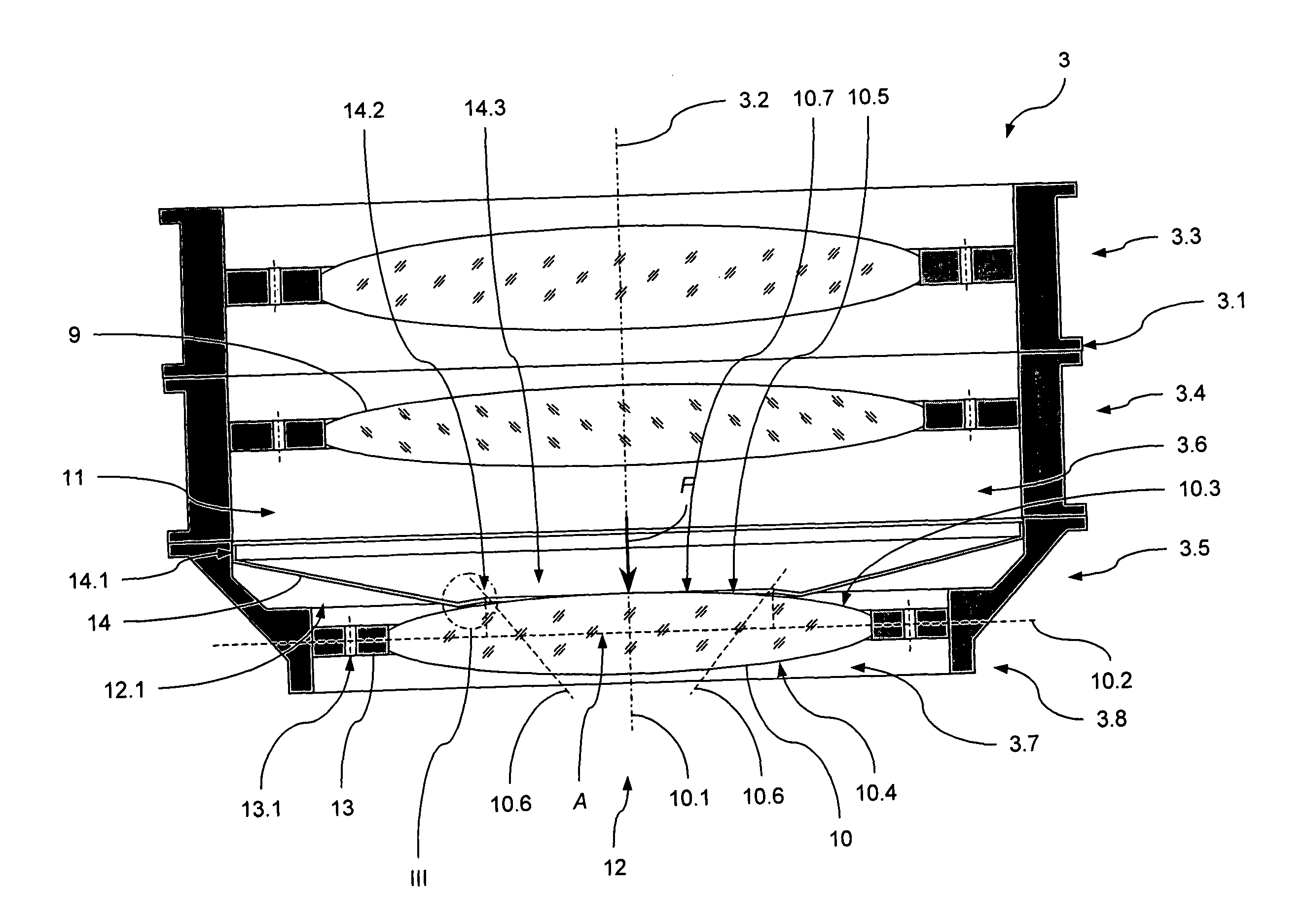
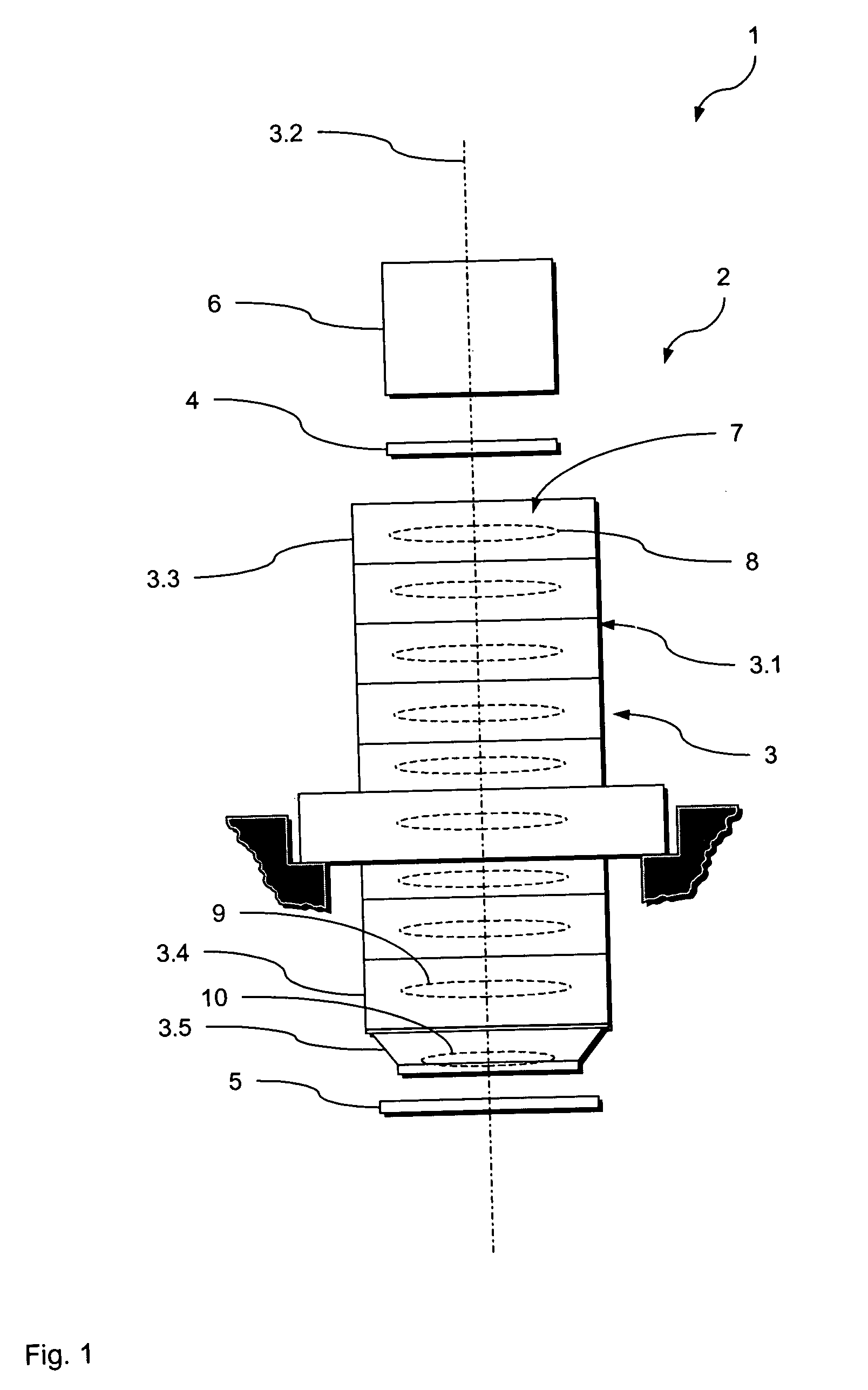
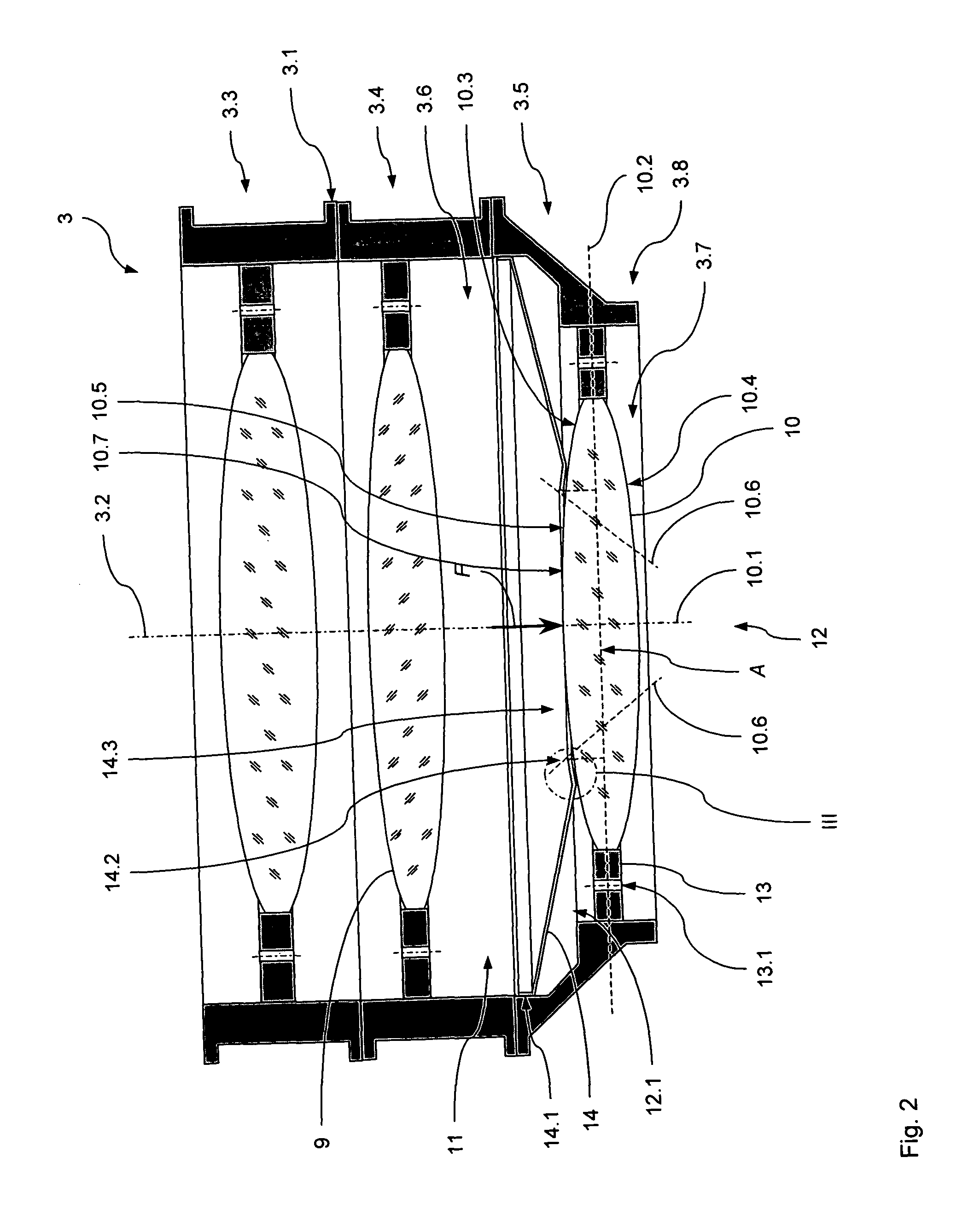
[0036]In the following, a first preferred embodiment of an optical exposure apparatus 1 according to the present invention comprising an optical projection system 2 with an optical element unit 3 according to the present invention will be described with reference to FIGS. 1 to 3.

[0037]The optical exposure apparatus 1 is adapted to transfer an image of a pattern formed on a mask 4 onto a substrate 5. To this end, the optical exposure apparatus 1 comprises an illumination system 6 illuminating the mask 4 and the optical element unit 3. The optical element unit 3 projects the image of the pattern formed on the mask 4 onto the substrate 5, e.g. a wafer or the like.

[0038]To this end, the optical element unit 3 holds an optical element group 7. This optical element group 7 is held within a housing 3.1 of the optical element unit 3. The optical element group 7 comprises a number of optical elements 8 and optical elements 9 and 10, such as lenses, mirrors or the like. These optical elements...

second embodiment

[0083]In the following, a second preferred embodiment of an optical exposure apparatus 101 according to the present invention comprising an optical projection system 102 with an optical element unit 103 according to the present invention will be described with reference to FIGS. 5 and 6.

[0084]The optical exposure apparatus 101 is adapted to transfer an image of a pattern formed on a mask 104 onto a substrate 105. To this end, the optical exposure apparatus 101 comprises an illumination system 106 illuminating the mask 104 and the optical element unit 103. The optical element unit 103 projects the image of the pattern formed on the mask 4 onto the substrate 105, e.g. a wafer or the like.

[0085]To this end, the optical element unit 103 holds an optical element group 107. This optical element group 107 is held within a housing 103.1 of the optical element unit 103. The optical element group 107 comprises a number of optical elements 108 and optical elements 109 and 110, such as lenses, ...

third embodiment

[0093]In the following, a third preferred embodiment of an optical exposure apparatus 201 according to the present invention comprising an optical projection system 202 with an optical element unit 203 according to the present invention will be described with reference to FIGS. 7 to 9.

[0094]The optical exposure apparatus 201 is adapted to transfer an image of a pattern formed on a mask 204 onto a substrate 205. To this end, the optical exposure apparatus 201 comprises an illumination system 206 illuminating the mask 204 and the optical element unit 203. The optical element unit 203 projects the image of the pattern formed on the mask 4 onto the substrate 205, e.g. a wafer or the like.

[0095]To this end, the optical element unit 203 holds an optical element group 207. This optical element group 207 is held within a housing 203.1 of the optical element unit 203. The optical element group 207 comprises a number of optical elements 208 and optical elements 209 and 210, such as lenses, mi...


PUM


Abstract

An optical element unit is provided comprising an optical element group for projecting light along an optical axis of the optical element group and a housing having an inner housing part partly defining a first space and a light passageway between the inner housing part and a second space. The inner housing part receives the optical element group. The optical element group comprises an ultimate optical element located in the region of the light passageway. A load-relieving device is provided adjacent to the ultimate optical element, the load relieving device partly defining the first space and the second space and at least partly relieving the ultimate optical element from loads resulting from pressure differences between the first space.

Description

CROSS-REFERENCE TO RELATED APPLICATIONS[0001]The present application is claiming priority of U.S. Provisional Patent Application No. 60 / 659,845, filed Mar. 9, 2005, the content of which is herein incorporated by reference.BACKGROUND OF THE INVENTION[0002]1. Field of the Invention[0003]The present invention relates to optical element units used in exposure processes, in particular to optical element units of microlithography systems. It further relates to optical exposure apparatuses comprising such optical element units. Furthermore, it relates to methods of manufacturing such optical element units. The invention may be used in the context of photolithography processes for fabricating microelectronic devices, in particular semiconductor devices, or in the context of fabricating devices, such as masks or reticles, used during such photolithography processes.[0004]2. Description of the Related Art[0005]Typically, the optical systems used in the context of fabricating microelectronic d...

Claims


Application Information

Patent Timeline
Patent Type & Authority Patents(United States)
IPC IPC(8): G02B15/14G02B7/02
CPCG03G15/0409G02B7/021G02B7/023G02B7/182G03F7/7015
Inventor LIPPERT, JOHANNES
Owner CARL ZEISS SMT GMBH
Why Eureka
Try Eureka