Optical element module

a technology of optical elements and modules, applied in the field of optical element modules, can solve the problems of reducing the rigidity of the support system, increasing stresses, and the likely inability of adhesives to provide a desirable long-term stable and rigid connection, and achieve good and long-term reliable imaging properties of the optical system

Inactive Publication Date: 2011-07-26
CARL ZEISS SMT GMBH
View PDF9 Cites 0 Cited by
  • Summary
  • Abstract
  • Description
  • Claims
  • Application Information

AI Technical Summary

Benefits of technology

[0012]It is thus an object of the invention to, at least to some extent, overcome the above disadvantages and to provide good and long term reliable imaging properties of an optical system used in an exposure process.
[0013]It is a further object of the invention to increase imaging accuracy of an optical system used in an exposure process by increasing the rigidity of the support mechanism for an optical element of the optical system.
[0014]It is a further object of the invention to increase imaging accuracy of an optical system used in an exposure process by reducing the deformations introduced into an optical element of the optical system via its support structure.
[0016]With this configuration, the direct connection between the optical element and the optical element holder in a wide contact area provides for a maximum rigidity at the interface between the optical element and the optical element holder. In particular, the rigidity at the interface is high in a direction perpendicular to the contact area. The mutual adaptation of the coefficients of thermal expansion, in turn, allows for such a direct connection without the risk of an excessive introduction of stresses into said interface and the optical element which would otherwise occur with such large contact areas due to differences in the thermal expansion behavior of the coupled parts.
[0018]A further advantage of the direct connection between the optical element an the optical element holder lies within the fact that the interface between the optical element an the optical element holder is or may be easily sealed. Thus, the advantages of the invention come to their full effect in applications where, in addition to the improved rigidity and deformation behavior, fluid tightness properties play an important role. Such applications may be so called immersion applications as they play an increasingly important role in photolithography processes for fabricating microelectronic devices. Here, typically, the last optical element of the optical system adjacent to the wafer and the part of the wafer to be currently worked on are immersed in an immersion fluid to achieve a numerical aperture NA>1.

Problems solved by technology

However, they have the disadvantage that they also reduce the rigidity of the support system.
To deal with this effect, the rigidity of the uncoupling elements might be increased, but this would reduce their deformation uncoupling abilities leading to increased stresses and, thus, the deformations introduced into the optical element.
However, the small contact pins as well as the layers of adhesive are likely not to provide for a desirable long term stable and rigid connection between the optical element and the support structure.
A further problem that arises with the three point support disclosed in this document is the wave like deformation introduced into the optical element due to the local concentration of the reaction forces to the gravitational forces acting on the optical element.

Method used


Image

  • Optical element module
  • Optical element module
  • Optical element module

Examples


first embodiment

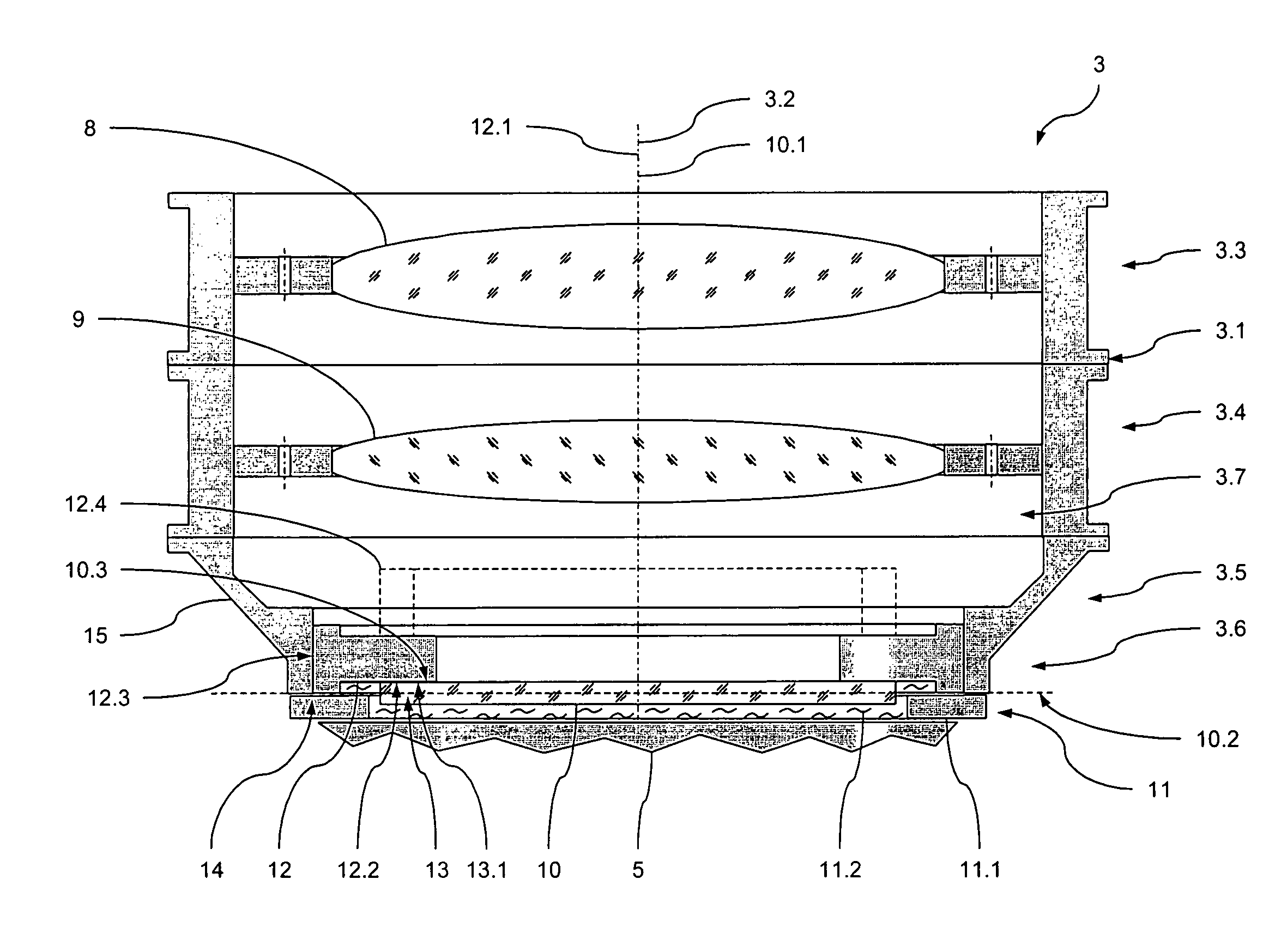
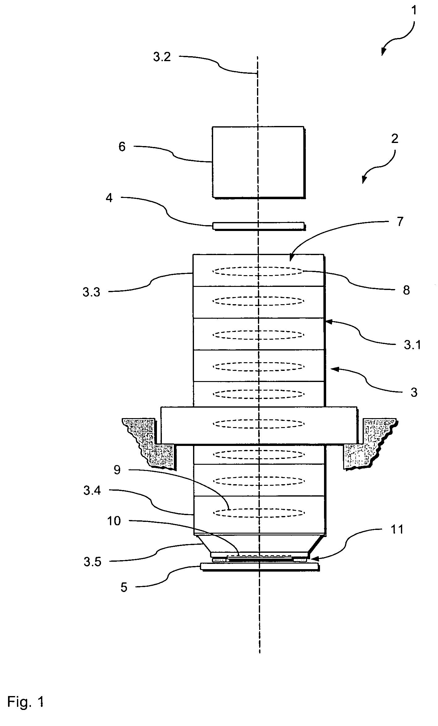
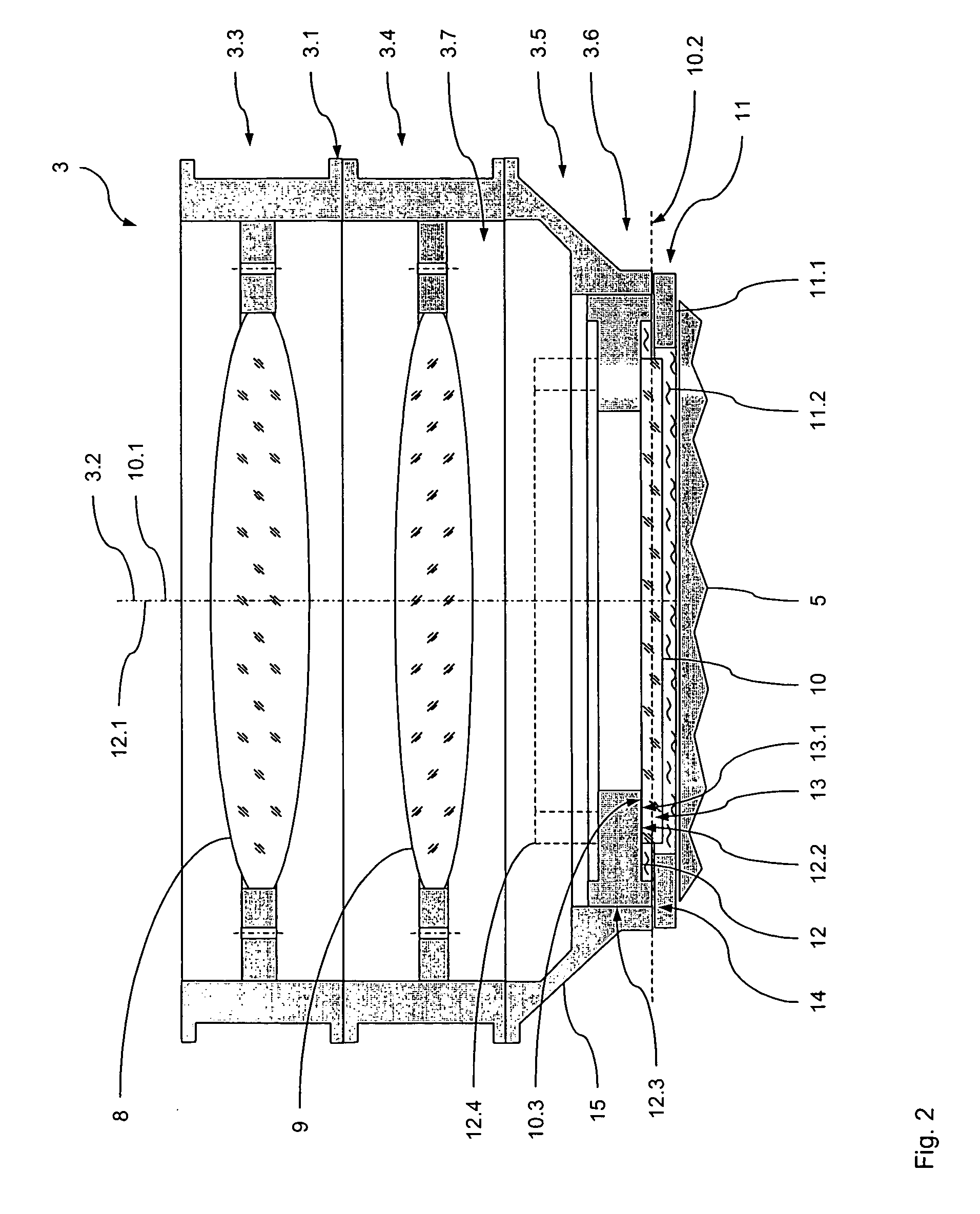
[0034]In the following, a first preferred embodiment of an optical exposure apparatus 1 according to the invention comprising an optical projection system 2 with an optical element unit 3 according to the invention will be described with reference to FIGS. 1 and 2.

[0035]The optical exposure apparatus 1 is adapted to transfer an image of a pattern formed on a mask 4 onto a substrate 5. To this end, the optical exposure apparatus 1 comprises an illumination system 6 illuminating said mask 4 and the optical element unit 3. The optical element unit 3 projects the image of the pattern formed on the mask 4 onto the substrate 5, e.g. a wafer or the like.

[0036]To this end, the optical element unit 3 holds an optical element group 7. This optical element group 7 is held within a housing 3.1 of the optical element unit 3. The optical element group 7 comprises a number of optical elements 8 and optical elements 9 and 10 such as lenses, mirrors or the like. These optical elements 8 to 10 are al...

second embodiment

[0070]In the following, a second preferred embodiment of an optical element module 103.5 according to the invention will be described with reference to FIGS. 1 and 4. In this embodiment, the optical element module 103.5 replaces the optical element module 3.5 within the exposure apparatus 1 of FIG. 1.

[0071]FIG. 4 shows a schematic sectional representation of the last optical element module 103.5 of the optical element unit 3. As can be seen from FIG. 4, the last optical element module 103.5 forming the exit end 3.6 of the optical element unit 3 comprises an ultimate optical element in the form of a lens 110 and an optical element holder 112 holding the lens 110.

[0072]The lens 110 is rotationally symmetric having a first axis of symmetry 110.1 essentially coinciding with the optical axis 3.2 of the optical element unit 3. The lens 110 mainly extends in a first plane 110.2 perpendicular to said first axis of symmetry 110.1.

[0073]The optical element holder is formed by a ring shaped fr...

third embodiment

[0089]In the following, a third preferred embodiment of an optical element module 203.5 according to the invention will be described with reference toFIGS. 1 and 5. In this embodiment, the optical element module 203.5 replaces the optical element module 3.5 within the exposure apparatus 1 of FIG. 1.

[0090]FIG. 5 shows a schematic sectional representation of the last optical element module 203.5 of the optical element unit 3. As can be seen from FIG. 5, the last optical element module 203.5 forming the exit end 3.6 of the optical element unit 3 comprises an ultimate optical element in the form of a plane parallel plate 210 and an optical element holder 212 holding the plane parallel plate 210.

[0091]The plane parallel plate 210 is rotationally symmetric having a first axis of symmetry 210.1 essentially coinciding with the optical axis 3.2 of the optical element unit 3. The plate 210 mainly extends in a first plane 210.2 perpendicular to said first axis of symmetry 210.1.

[0092]The optic...


PUM


Abstract

There is provided an optical element module comprising a first optical element and an optical element holder. The first optical element has a first coefficient of thermal expansion. The optical element holder holds the first optical element and has a second coefficient of thermal expansion, the second coefficient of thermal expansion being adapted to the first coefficient of thermal expansion. The optical element is directly contacting the optical element holder in a wide contact area. The contact area is defined by a first contact surface of the first optical element and a second contact surface of the optical element holder, wherein the second contact surface matches the first contact surface. Thus, favorable rigidity and deformation behavior is provided.

Description

CROSS-REFERENCE TO RELATED APPLICATIONS[0001]The present application is claiming priority of U.S. Provisional Patent Application No. 60 / 685,864, filed May 31, 2005, the content of which is herein incorporated by reference.BACKGROUND OF THE INVENTION[0002]The invention relates to optical element modules used in exposure processes, in particular to optical element modules of microlithography systems. It further relates to optical element units comprising such optical element modules. It also relates to optical exposure apparatuses comprising such optical element units. Furthermore, it relates to a method of holding an optical element as well as a method of manufacturing such optical element modules. The invention may be used in the context of photolithography processes for fabricating microelectronic devices, in particular semiconductor devices, or in the context of fabricating devices, such as masks or reticles, used during such photolithography processes.[0003]Typically, the optical...

Claims


Application Information

Patent Timeline
Patent Type & Authority Patents(United States)
IPC IPC(8): G02B7/02
CPCG02B7/008G02B7/028G03F7/70825G03F7/70891
Inventor KUGLER, JENSWEBER, ULRICHGELLRICH, BERNHARDKWAN, YIM-BUN PATRICKDEUFEL, PETER
Owner CARL ZEISS SMT GMBH
Why Eureka
Try Eureka