Semiconductor device having trench gate structure

a technology of semiconductor devices and gate structures, which is applied in the direction of semiconductor devices, diodes, electrical devices, etc., can solve the problems of difficult integration and worsening of ions

Inactive Publication Date: 2011-06-07
RENESAS ELECTRONICS CORP
View PDF3 Cites 1 Cited by
  • Summary
  • Abstract
  • Description
  • Claims
  • Application Information

AI Technical Summary

Benefits of technology

[0016]Thereby, since reduction in a channel length is very slight, increase of the Ron is effectively suppressed. In addition, since it is possible to centralize an avalanche current on a diode region (anode region 6P+), it is possible to prevent breakdown of a device and it becomes possible to secure the avalanche resistance.
[0017]According to the present invention, it is possible to provide a vertical MOSFET which has striped trench gate structure which can secure avalanche resistance without increasing Ron.

Problems solved by technology

Nevertheless, the inventors have found out that there are the following issues in these prior arts.
Thus, when the Ron is emphasized, avalanche resistance is reduced, and when avalanche resistance is secured, the Ron gets worse, which are in a trade-off relation.
In addition, in the structure disclosed in Williams, the following problems arise.
For this reason, since it is not possible to narrow the space between the gate trenches 91, there arises a problem that integration is difficult.

Method used


Image

  • Semiconductor device having trench gate structure
  • Semiconductor device having trench gate structure
  • Semiconductor device having trench gate structure

Examples


first embodiment

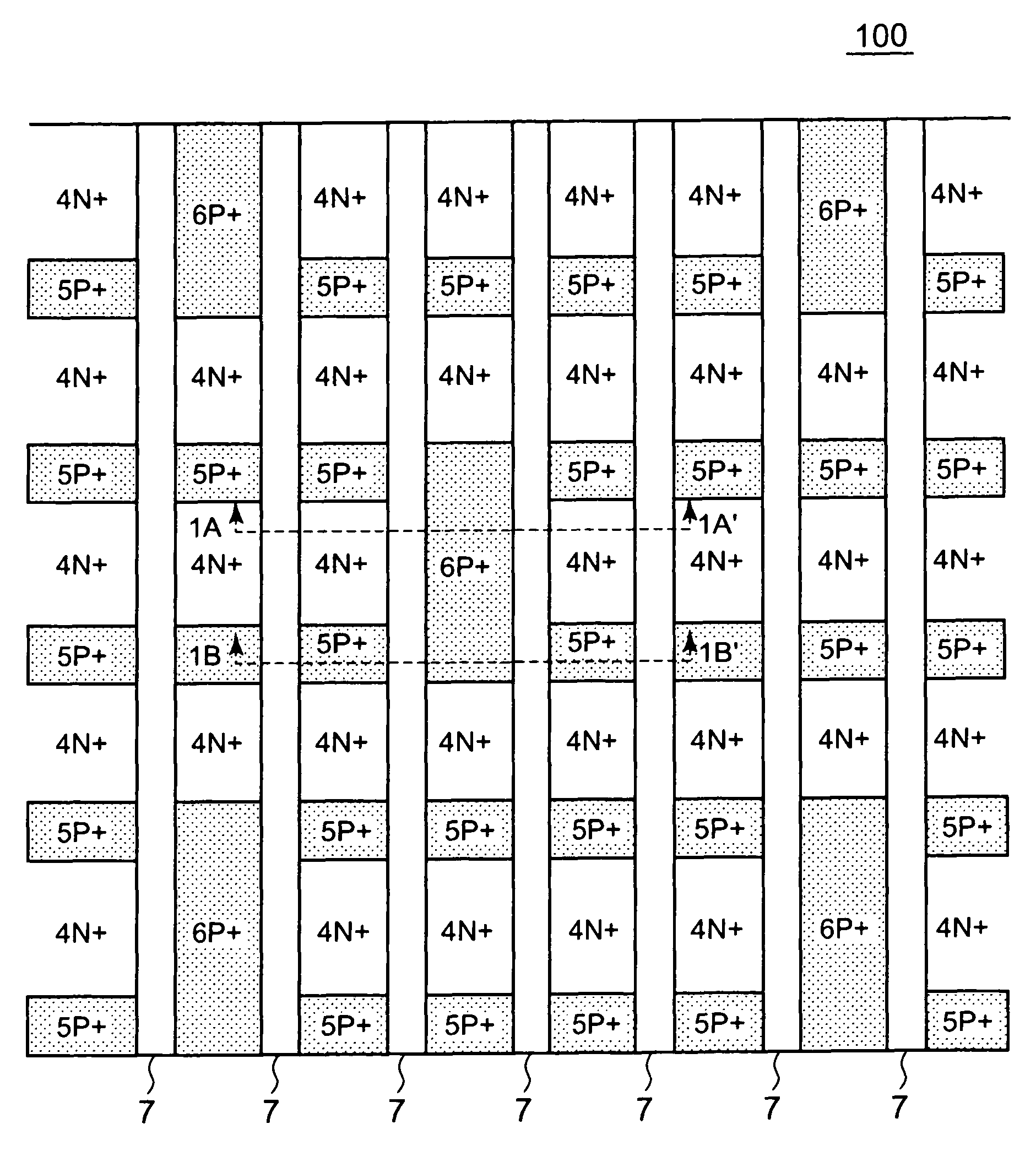
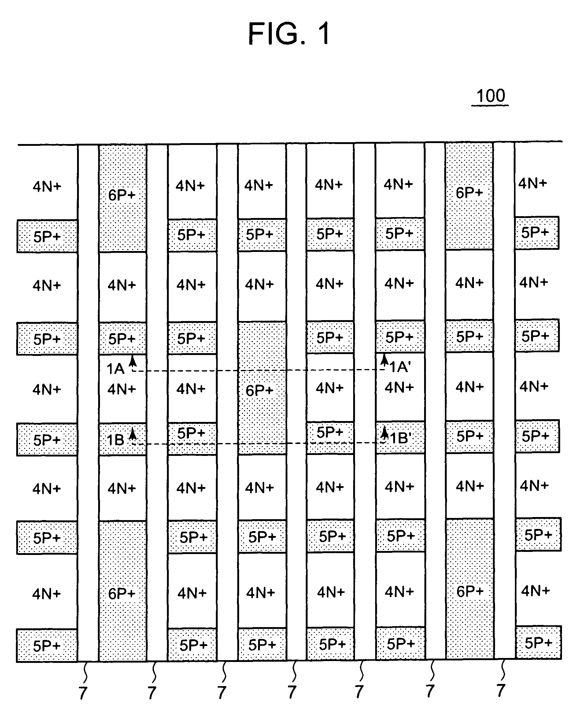
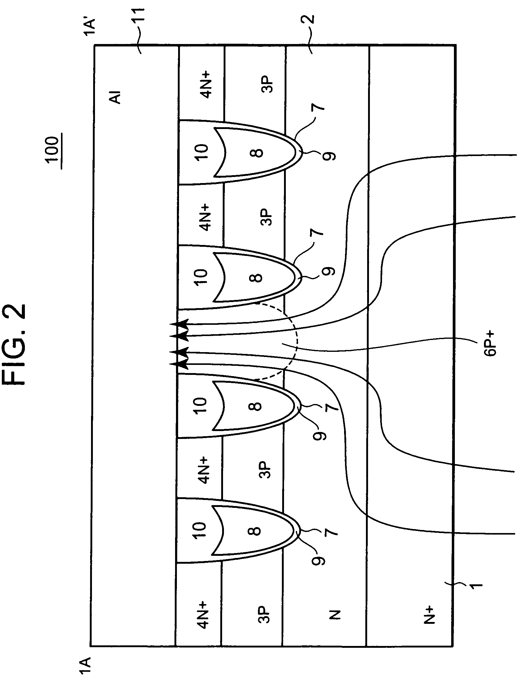
[0035]Construction of a semiconductor device according to a first embodiment of the present invention will be described with reference to FIG. 1 to FIG. 3. FIG. 1 is a schematic plan view showing planar structure of an N channel type vertical MOSFET 100 which is an example of the semiconductor device according to the first embodiment. FIG. 2 is a schematic sectional view taken along line 1A-1A′ of FIG. 1. FIG. 3 is a schematic sectional view taken along line 1B-1B′ of FIG. 1.

[0036]As shown in FIG. 1, the vertical MOSFET 100 has gate trenches 7 arranged in stripes. A plurality of gate trenches 7 are formed in a MOSFET cell region. In addition, these gate trenches 7 may be connected mutually in a peripheral region and become a single trench. In addition, the plurality of gate trenches 7 may not be connected mutually even in a peripheral region and remain being plural.

[0037]Between the gate trenches 7, N+ source regions 4N+ and P+ base contact regions 5P+ are formed. The N+ source regi...

second embodiment

[0049]Construction of a semiconductor device according to a second embodiment of the present invention will be described with reference to FIG. 4. FIG. 4 is a schematic plan view showing planar structure of an N channel type vertical MOSFET 110 which is an example of the semiconductor device according to the second embodiment. In the vertical MOSFET 110, a different point from the vertical MOSFET 100 shown in FIG. 1 is a formation position of a diode region (anode region 6P+). In addition, in FIG. 4, the same reference numerals are assigned to the same components as those in FIGS. 1 to 3, and their descriptions are omitted.

[0050]In the vertical MOSFET 100, a diode region (anode region 6P+) is formed in a part of arbitrary two P+ base contact regions 5P+ and one N+ source region 4N+ sandwiched between the two adjacent P+ base contact regions 5P+. In the vertical MOSFET 110, the diode region (anode region 6P+) is formed so as to stride one P+ base contact region 5P+.

[0051]Specifically...

third embodiment

[0054]Construction of a semiconductor device according to a third embodiment of the present invention will be described with reference to FIG. 5. FIG. 5 is a schematic plan view showing planar structure of an N channel type vertical MOSFET 120 which is an example of the semiconductor device according to the third embodiment. In the vertical MOSFET 120, a different point from the vertical MOSFET 100 shown in FIG. 1 is a formation position of a diode region (anode region 6P+). In addition, in FIG. 5, the same reference numerals are assigned to the same components as those in FIGS. 1 to 3, and their descriptions are omitted.

[0055]As shown in FIG. 5, in the vertical MOSFET 120, a diode region (anode region 6P+) is formed between arbitrary two adjacent gate trenches 7. In other words, all of the N+ source region 4N+ and the P+ base contact region 5p+ of an arbitrary array are replaced with a single anode region 6P+.

[0056]Specifically, as shown in FIG. 5, the vertical MOSFET 120 has the g...


PUM


Abstract

The present invention provides a vertical MOSFET which has striped trench gate structure which can secure avalanche resistance without increasing Ron. A vertical MOSFET 100 comprises a plurality of gate trenches 7 which is arranged in stripes, an array which is sandwiched with the plurality of gate trenches 7 and includes N+ source regions 4N+ and P+ base contact regions 5P+, and a diode region (anode region 6P+) which is formed so as to contact with two gate trenches 7. The N+ source regions 4N+ and the base contact regions 5P+ are alternately arranged along a longitudinal direction of the gate trench 7. Size of the diode region (anode region 6P+) corresponds to at least one of the N+ source regions 4N+ and two of the P+ base contact regions 5P+.

Description

CROSS-REFERENCE TO RELATED APPLICATIONS[0001]This application is based upon, claims the benefit of priority of, and incorporates by reference the contents of Japanese Patent Application No. 2007-242011 filed on Sep. 19, 2007.BACKGROUND[0002]1. Field of the Invention[0003]The present invention relates to a semiconductor device, and in particular, to a semiconductor device which has trench gate structure.[0004]2. Description of the Related Art[0005]In a vertical metal-oxide semiconductor field-effect transistor (MOSFET) with striped trench gate structure, avalanche resistance is influenced by a width, a space, and a gross area of a P+ base contact region. The narrower the space of the P+ base contact region is, the more avalanche resistance improves. On the other hand, since a channel region decreases, the on-resistance (Ron) which is one of the performance indices of a vertical MOSFET increases. Hence, it is required to achieve structure of enhancing the avalanche resistance with sec...

Claims


Application Information

Patent Timeline
Patent Type & Authority Patents(United States)
IPC IPC(8): H01L29/76H01L31/119H01L29/94H01L31/062H01L31/113H01L29/78
CPCH01L27/0727H01L29/0696H01L29/7813H01L29/7808H01L29/1095
Inventor YAMAMOTO, HIDEOKOBAYASHI, KENYAKANEKO, ATSUSHI
Owner RENESAS ELECTRONICS CORP
Why Eureka
Try Eureka