Imager methods, apparatuses, and systems providing a skip mode with a wide dynamic range operation

a wide dynamic range, image sensor technology, applied in the field of image sensors, can solve the problems of reducing readout time, cmos image sensors are unable to achieve this high dynamic range, and image sensors are generally unable to capture all details

Active Publication Date: 2011-06-07
MICRON TECH INC
View PDF16 Cites 9 Cited by
  • Summary
  • Abstract
  • Description
  • Claims
  • Application Information

AI Technical Summary

Problems solved by technology

Typical CMOS image sensors are unable to attain this high dynamic range due to the limitations of the full well and noise floor.
Consequently, a typical image sensor will generally be unable to capture all details from deep shadows to bright highlights of a scene.
Skip modes are used to readout only a portion of an image array which decreases the readout time but also reduces output resolution in a given field of view.
Typical column skip mode operations, however, will leave a substantial part of the column readout circuit unused, e.g., half and three-fourths for “2×” and “4×” skip modes, respectively.

Method used


Image

  • Imager methods, apparatuses, and systems providing a skip mode with a wide dynamic range operation
  • Imager methods, apparatuses, and systems providing a skip mode with a wide dynamic range operation
  • Imager methods, apparatuses, and systems providing a skip mode with a wide dynamic range operation

Examples


Embodiment Construction

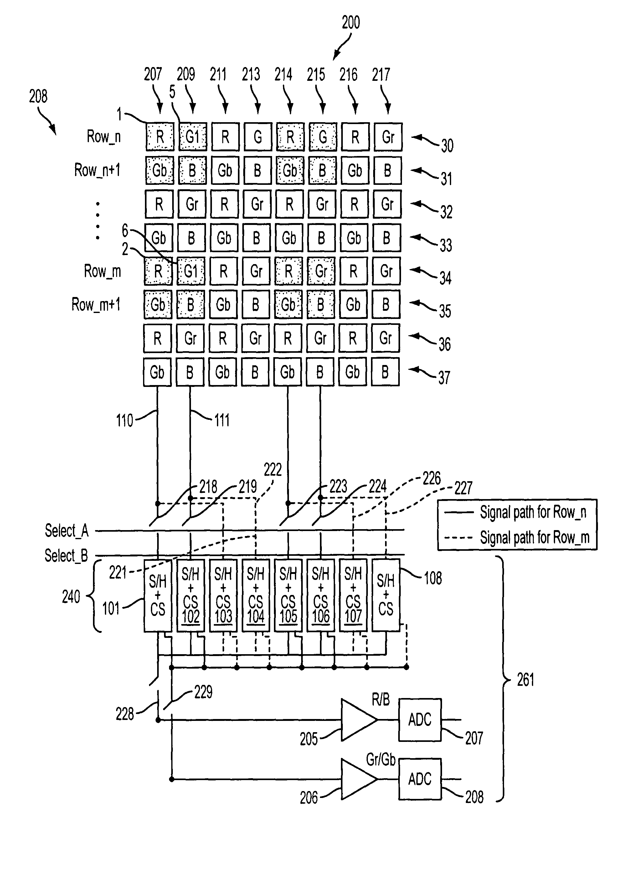
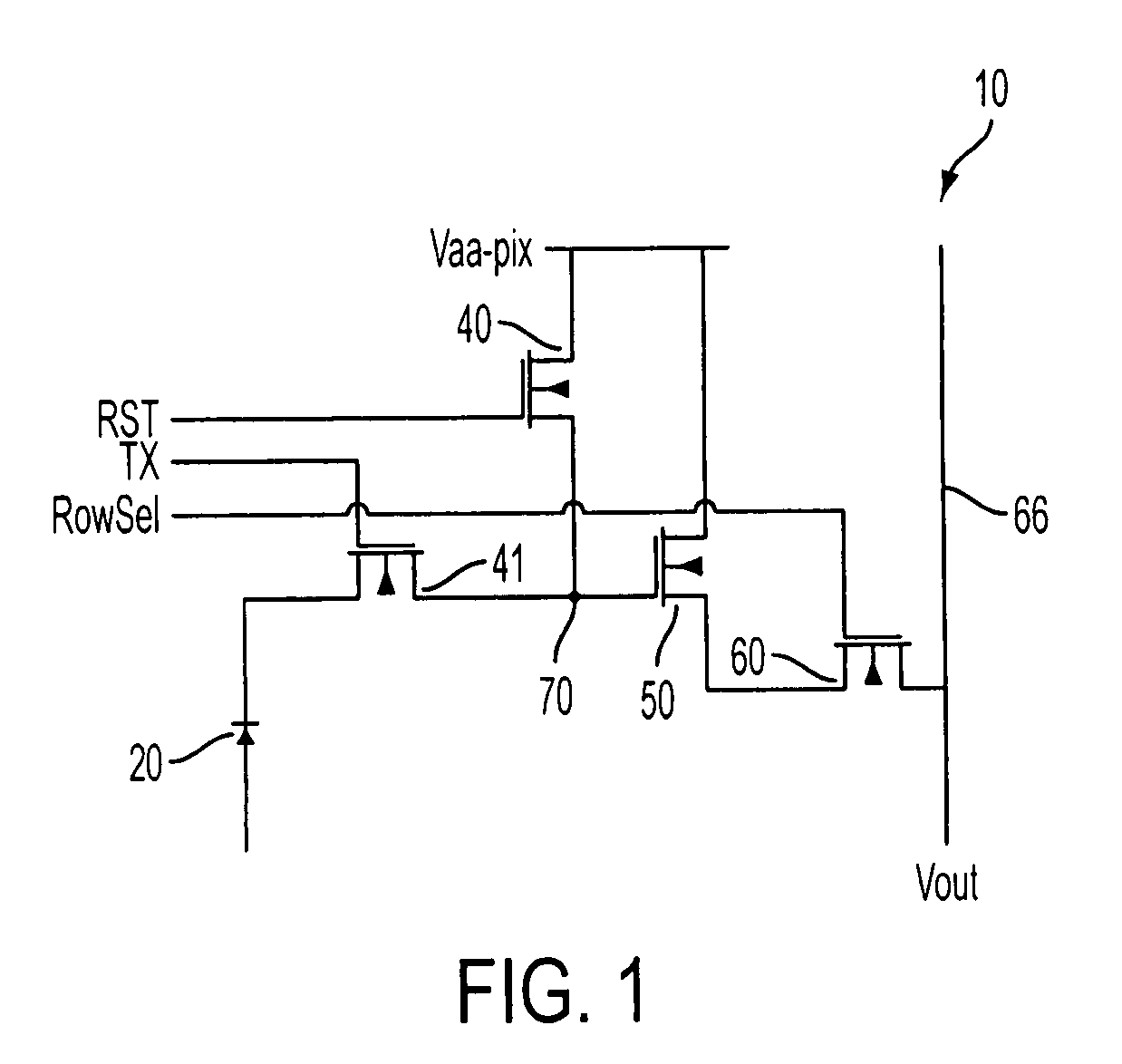
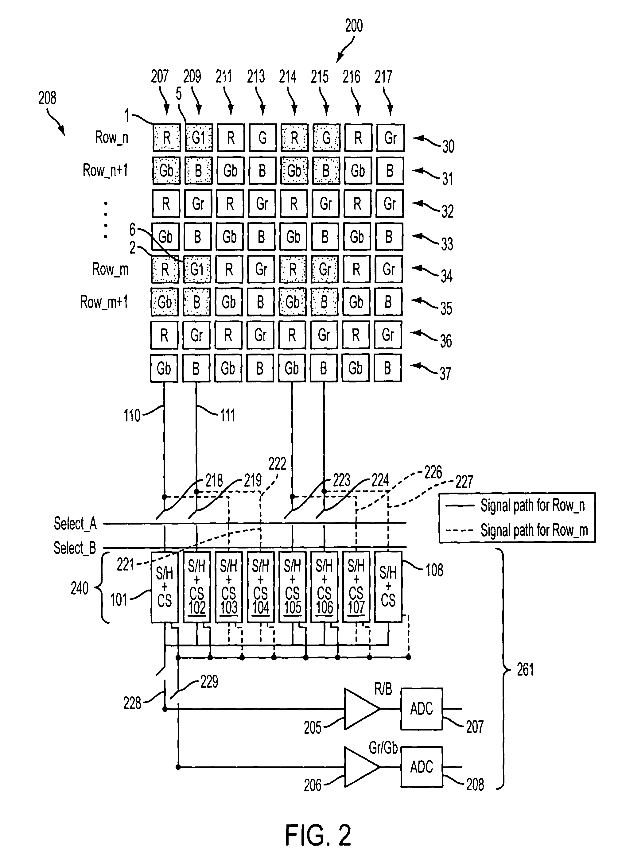
[0019]In the following detailed description, reference is made to the accompanying drawings, which form a part hereof and illustrate specific embodiments in which the invention may be practiced. In the drawings, like reference numerals describe substantially similar components throughout the several views. These embodiments are described in sufficient detail to enable those skilled in the art to practice them, and it is to be understood that other embodiments may be utilized, and that structural, logical and electrical changes may be made.

[0020]The term “pixel” refers to a picture element unit cell containing at least a photosensor for converting electromagnetic radiation to an electrical signal. For purposes of illustration, a representative pixel is illustrated in the figures and description herein, and typically fabrication of all pixels in a pixel array will proceed simultaneously in a similar fashion.

[0021]Although the following embodiments are described herein with reference t...


PUM


Abstract

Methods, apparatuses and systems provide a high dynamic range mode of operation for an image sensor when operating in a skip mode where certain pixels of an array are not readout. Multiple integration periods are employed in the skip mode with selected pixels being readout through circuits associated with pixels that are not readout.

Description

FIELD OF THE INVENTION[0001]Embodiments of the invention relate generally to image sensors and more particularly, to wide dynamic range image sensors.BACKGROUND OF THE INVENTION[0002]Image sensors, such as complementary metal oxide semiconductors (CMOS), include a focal plane array of pixels. Each pixel in a CMOS image sensor, for instance, includes a photosensor, such as, a photogate, a photoconductor or a photodiode overlying a substrate. A readout circuit is provided for each pixel and includes at least a source follower transistor and a row select transistor for coupling the source follower transistor to a column output line. A pixel also typically has a floating diffusion region, connected to a gate of the source follower transistor.[0003]A pixel's photosensor collects photons (incoming light) and converts the photons into an electrical charge. The image sensor may also include a transfer transistor for transferring the electrical charge generated by the photosensor to the floa...

Claims


Application Information

Patent Timeline
Patent Type & Authority Patents(United States)
IPC IPC(8): H04N3/14H04N5/335H04N1/04H04N5/345H04N5/355H04N5/374H04N9/07
CPCH04N3/1562H04N5/23245H04N5/335H04N9/045H04N5/3458H04N5/35581H04N5/3742H04N5/3456H04N23/667H04N25/445H04N25/531H04N25/533H04N25/589H04N25/00H04N25/767H04N25/447H04N25/70H04N25/134
Inventor XU, CHEN
Owner MICRON TECH INC
Why Eureka
Try Eureka