Circuit and method for recovering clock data in highly integrated semiconductor memory apparatus

a memory device and circuit technology, applied in the field of high-integrated semiconductor devices, can solve the problems of increasing the number of data transmission channels increasing the possibility of semiconductor memory device malfunction, and increasing the power consumption of the semiconductor memory devi

Active Publication Date: 2011-06-21
SK HYNIX INC
View PDF10 Cites 4 Cited by
  • Summary
  • Abstract
  • Description
  • Claims
  • Application Information

AI Technical Summary

Benefits of technology

[0014]Embodiments of the present invention are directed to providing an apparatus and method for improving a clock data recover (CDR) circuit of a highly integrated semiconductor memory apparatus so as to be usefully used in a highly integrated semiconductor apparatus, an electronic device, and an electronic system, the apparatus and method being configured to recover clock data using a small space and power by grouping signal input / output pads and allowing each of the groups to share a clock data recovery (CDR) circuit.

Problems solved by technology

In this case, the semiconductor memory device cannot normally operate according to the data and clock signals, and thus the possibility of malfunction of the semiconductor memory device increases.
Therefore, the number of data transmission channels of the semiconductor memory device may be limited, or the power consumption of the semiconductor memory device may be increased due to the CDR operation.

Method used


Image

  • Circuit and method for recovering clock data in highly integrated semiconductor memory apparatus
  • Circuit and method for recovering clock data in highly integrated semiconductor memory apparatus
  • Circuit and method for recovering clock data in highly integrated semiconductor memory apparatus

Examples


Embodiment Construction

[0023]Hereinafter, circuit and method for recovering clock data in highly integrated semiconductor memory apparatus in accordance with the present invention will be described in detail with reference to the accompanying drawings.

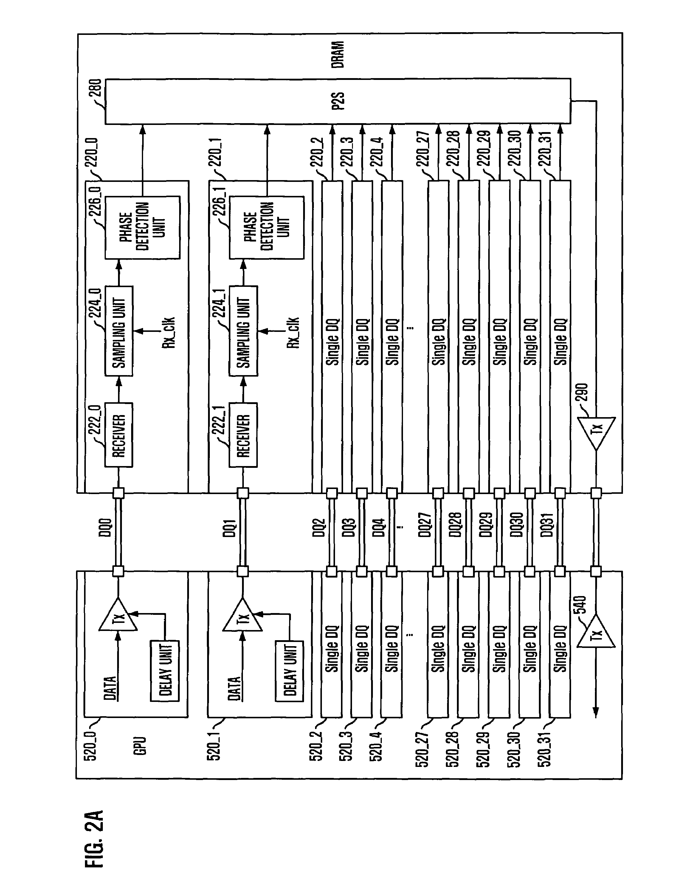
[0024]FIG. 2A is a block diagram illustrating a semiconductor memory apparatus and a data processing apparatus in accordance with an embodiment of the present invention.

[0025]Referring to FIG. 2A, the semiconductor memory apparatus may be a dynamic random access memory (DRAM). The semiconductor memory apparatus receives a plurality of parallel signals according to a receiving reference clock signal and detects phases of the signals. Then, the semiconductor memory apparatus converts the detection result into a serial signal. The data processing apparatus may be a general processing unit (GPU). The data processing apparatus detects a signal transmission state using the serial signal received from the semiconductor memory apparatus. Then, the data processing ap...


PUM


Abstract

Circuit and method for recovering clock data in highly integrated semiconductor memory apparatus includes a plurality of signal receiving units configured to receive signals through a plurality of input / output pads and transfer the signals according to a receiving reference clock, the signal receiving units being divided into groups, a plurality of phase detection units configured to detect phases of signals output from the groups of the signal receiving units, a plurality of phase detection control units configured to control the phase detection units so that the phase detection units sequentially detect the phases of the signals output from each of the groups of the signal receiving units and a notification unit configured to output signals output from the phase detection units.

Description

CROSS-REFERENCE TO RELATED APPLICATIONS[0001]The present invention claims priority of Korean patent application number 10-2007-0111482, filed on Nov. 2, 2007, which is incorporated by reference in its entirety.BACKGROUND OF THE INVENTION[0002]The present invention relates to a highly integrated semiconductor device, and more particularly, to a semiconductor memory device including a clock data recovery (CDR) circuit for recovering signals and data distorted during high-speed processing.[0003]Semiconductor memory devices are used for storing data in various systems such as a system composed of a plurality of semiconductor devices. When a data processing device, such as a central processing unit (CPU), requests or sends data, a semiconductor memory device outputs or stores the data based on address information received from the data processing device.[0004]As the operating speed of a semiconductor device system increases owing to the advance of semiconductor integrated circuit technol...

Claims


Application Information

Patent Timeline
Patent Type & Authority Patents(United States)
IPC IPC(8): G11C8/18
CPCH03H11/26G11C11/407G11C11/4096G11C11/4076
Inventor KIM, KYUNG-HOONBYEON, SANG-YEONCHOI, CHANG-KYU
Owner SK HYNIX INC
Why Eureka
Try Eureka