Enhanced integrated circuit package

a technology of integrated circuits and packaging materials, applied in the direction of electrical equipment, semiconductor devices, semiconductor/solid-state device details, etc., can solve the problems of uniform distance between adjacent wire bonds around the leadframe, and the problem of affecting the adhesion of the leadframe so as to improve the adhesion of the lead fingers of the lead frame to the molding material, and improve the adhesion of the lead fingers under selective plating.

Inactive Publication Date: 2011-07-05
BLONDWICH
View PDF6 Cites 4 Cited by
  • Summary
  • Abstract
  • Description
  • Claims
  • Application Information

AI Technical Summary

Benefits of technology

[0009]In a more preferred embodiment, at least one edge of the tip of the lead finger further includes a selectively etched pattern for increasing the surface area for adhesion to a molding material.
[0010]There are many advantages to the present invention, one of which is that the adhesion of the lead fingers of the lead frame to the molding material is greatly improved when selective plating and / or selective etching are applied. As the plating is selectively applied to only the center portion of the tips, more area of the metallic substrate is exposed to the molding material. Since lead frame material adheres to the molding material better than noble metals used at the bonding pad, the adhesion of the lead fingers under selective plating is improved. Furthermore, the selective etching manufacturing process also increases the surface area of the substrate for metal-to-molding-material adhesion. Thus, the overall reliability of the semiconductor package can also be improved.
[0011]Another advantage of the present invention is that the bleeding phenomenon of noble metal over the edge of the lead tips can be effectively eliminated. Since plating of noble metal in the present invention is only selectively applied to the center portion of the lead tip surface, but not to the edge of the tip surface, bleeding will not take place. Not only will the selective plating process conserve the consumption of noble metal, the absence of bleeding will also prevent the chance of electrical short-circuit between the lead tips.
[0012]Moreover, by selective etching of the top surfaces of the lead tips, the center of gravity of the lead tips of the lead fingers is lowered compared to conventional plating method, so that the likelihood that the lead tips will move or become misaligned during the manufacturing process is reduced. This ensures the reliability, productivity and consistency of the whole semiconductor package.

Problems solved by technology

Plating the entire surface area of the relative large, flat tabs created a plurality of problems, including, among other things, non-uniform distances between adjacent wire bonds around the leadframe.

Method used


Image

  • Enhanced integrated circuit package
  • Enhanced integrated circuit package
  • Enhanced integrated circuit package

Examples


Embodiment Construction

[0024]Various embodiment of the present invention will now be described more fully with reference to the accompanying drawings. The invention may, however, be embodied in many different forms and should not be construed as limited to the embodiments set forth herein; rather, the embodiments are provided so that this disclosure will be thorough and complete, and will fully convey the scope of the invention to those skilled in the art.

[0025]As used herein and in the claims, “comprising” means including the following elements but not excluding others; and “couple” or “connect” refer to electrical coupling or connection either directly or indirectly via one or more electrical means unless otherwise stated.

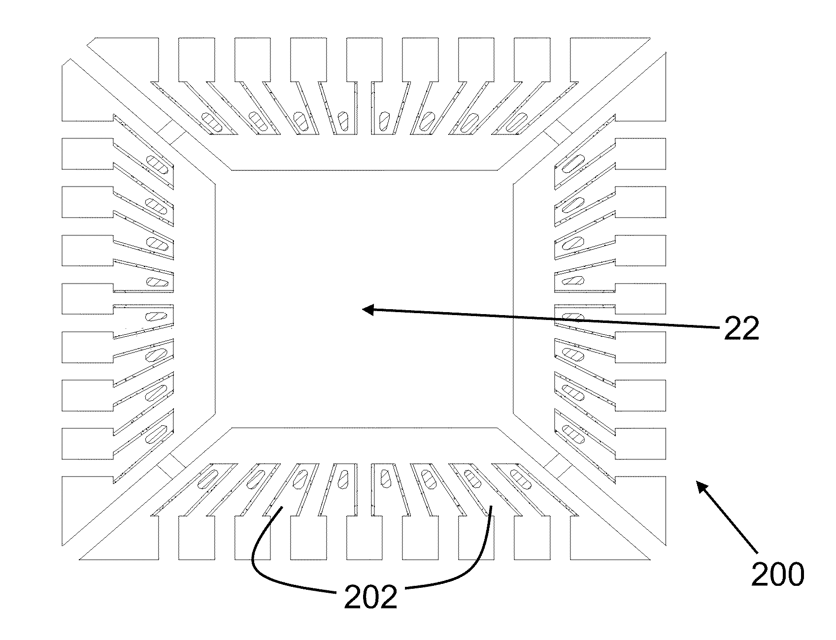
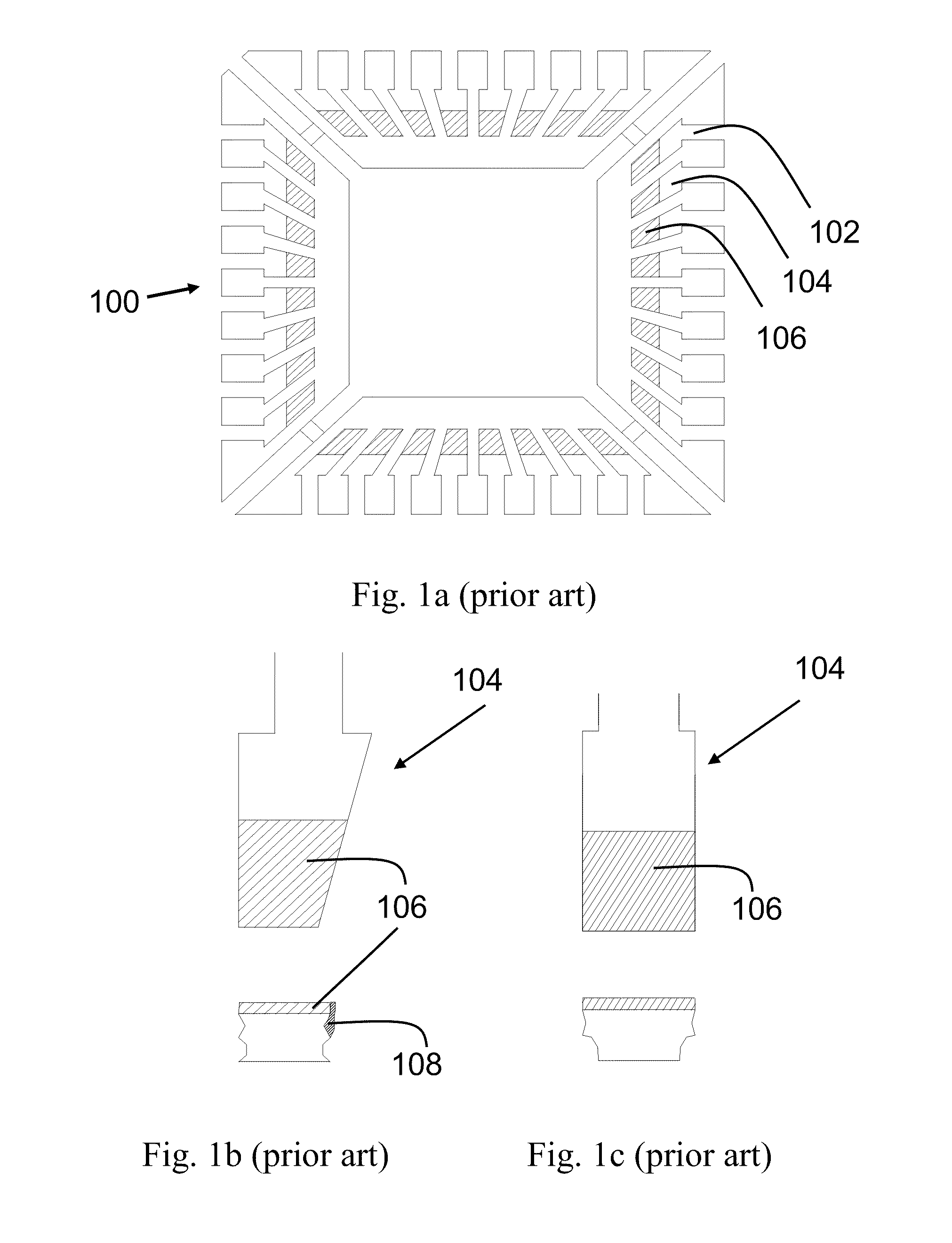
[0026]Referring now to FIG. 1a, a conventional lead frame 100 is shown having a plurality of lead fingers 102 extending along the periphery of the lead frame 100. Each of the lead fingers 102 has a lead tip 104 and each of the lead tips 104 has been plated to form a bonding pad 106 the...


PUM

PropertyMeasurementUnit
diameteraaaaaaaaaa
diameteraaaaaaaaaa
perimeteraaaaaaaaaa

Abstract

A semiconductor including a selectively plated lead frame is disclosed. The lead frame contains a die pad and a plurality of lead fingers, where each lead finger is formed with a bonding pad on the center portion of the lead finger by selective plating. The surface area of the lead finger material is increased so the adhesion to molding material is improved. The edges of the lead finger tips are half etched to further increase the surface area of lead finger material. A method of manufacturing the lead frame is also provided.

Description

CROSS-REFERENCE TO RELATED APPLICATION[0001]This application claims benefit under 35 U.S.C. §119(e) of U.S. Provisional Application having Ser. No. 61 / 185,968 filed Jun. 10, 2009, which is hereby incorporated by reference herein in its entirety.FIELD OF INVENTION[0002]This patent application relates generally to integrated circuit (IC) packaging technology and, in particular, but not by way of imitation, to IC packages having selectively etched internal lead tips.BACKGROUND OF INVENTION[0003]IC packages often incorporate IC chips mounted to lead frames. Lead frames are often formed from a metal sheet, such as, for example, copper or a copper alloy, by forming various patterns on a top surface thereof by, for example, a stamping and / or punching process or by an etching process. The IC chips are often mounted in a center region of the lead frame and electrically coupled to the lead frame via wire bonds from the IC chip to bonding areas disposed around the IC chip. Oftentimes, the bond...

Claims


Application Information

Patent Timeline
Patent Type & Authority Patents(United States)
IPC IPC(8): H01L23/495
CPCH01L21/4828H01L23/3142H01L23/49541H01L23/49548H01L23/49582Y10T29/49117H01L2224/48091H01L2224/48247H01L2924/01046H01L2924/01077H01L2924/01078H01L2924/01079H01L23/3107H01L2224/73265H01L2224/48465H01L2224/32245H01L24/48H01L2924/00014H01L2924/00H01L2924/14H01L2924/181H01L2924/00012H01L2224/45099H01L2224/45015H01L2924/207
Inventor LI, TUNG LOK
Owner BLONDWICH
Why Eureka
Try Eureka