CMOS devices having dual high-mobility channels

a high-mobility channel and cmos technology, applied in the field of semiconductor devices, can solve the problems of less than optimal drawbacks of the above-discussed method, etc., and achieve the effects of reducing threshold voltage, improving drive current of the nmos device, and reducing leakage curren

Inactive Publication Date: 2011-08-09
TAIWAN SEMICON MFG CO LTD
View PDF7 Cites 17 Cited by
  • Summary
  • Abstract
  • Description
  • Claims
  • Application Information

AI Technical Summary

Benefits of technology

[0011]The advantageous features of the present invention include improved drive currents for NMOS devices, and reduced threshold voltages and reduced leakage currents for PMOS devices.

Problems solved by technology

The CMOS devices formed using the above-discussed method, however, suffer from drawbacks.
The channel region of the NMOS device formed in NMOS region 4 has no strain coming from the underlying substrate, and thus the drive current of the NMOS device is less than optimal.

Method used


Image

  • CMOS devices having dual high-mobility channels
  • CMOS devices having dual high-mobility channels
  • CMOS devices having dual high-mobility channels

Examples


Embodiment Construction

[0015]The making and using of the presently preferred embodiments are discussed in detail below. It should be appreciated, however, that the present invention provides many applicable inventive concepts that can be embodied in a wide variety of specific contexts. The specific embodiments discussed are merely illustrative of specific ways to make and use the invention, and do not limit the scope of the invention.

[0016]A method for forming a complementary metal-oxide-semiconductor (CMOS) structure is provided. The intermediate stages of manufacturing embodiments of the present invention are illustrated. Throughout various views and illustrative embodiments of the present invention, like reference numbers are used to designate like elements.

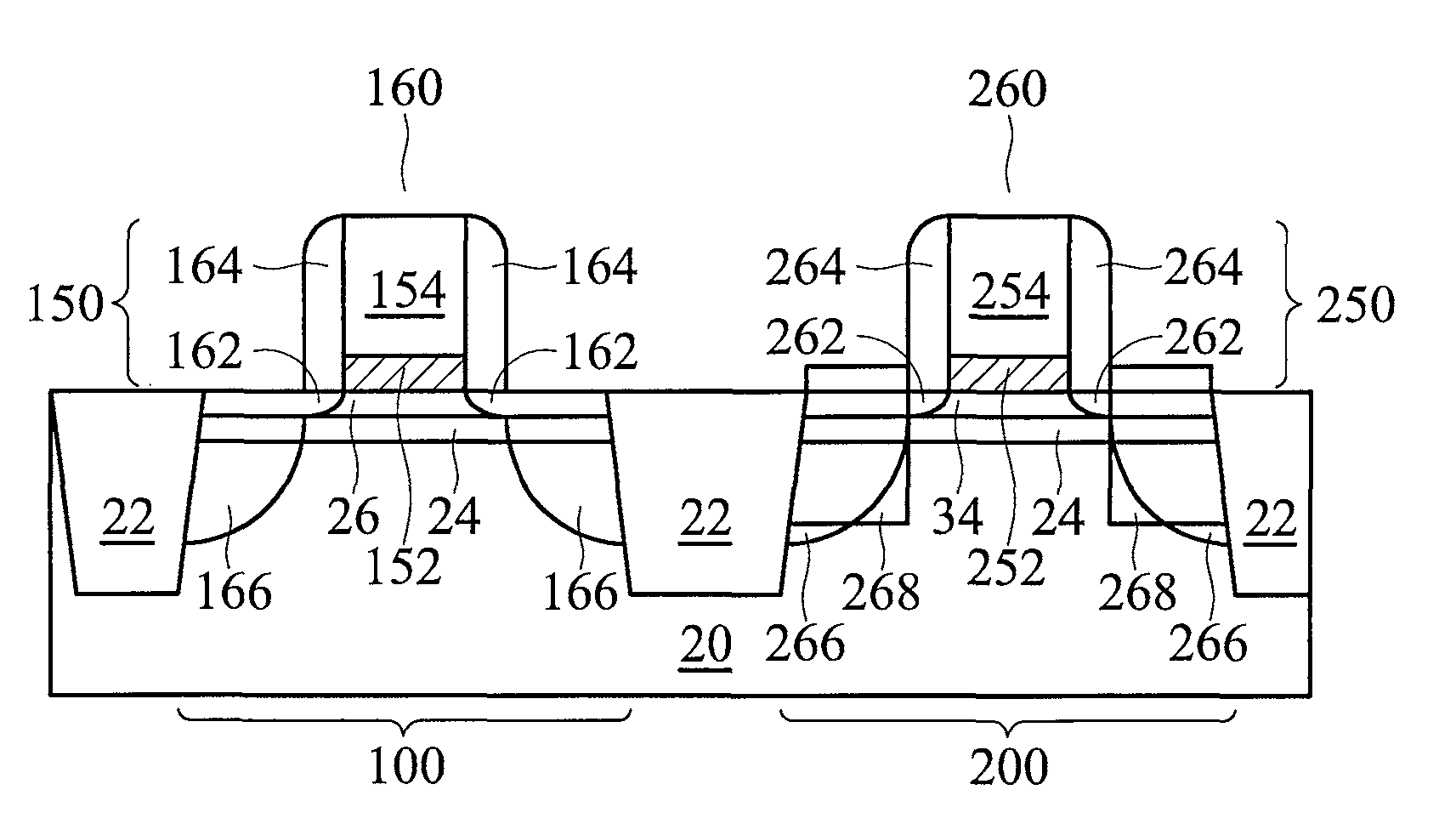
[0017]Referring to FIG. 6, semiconductor substrate 20 is provided, which may be formed of commonly used semiconductor materials and structures such as bulk silicon, silicon-on-insulator (SOI), and the like. Semiconductor substrate 20 includes NMOS r...


PUM


Abstract

A method for forming a semiconductor structure includes providing a semiconductor substrate including a first region and a second region; and forming a first and a second metal-oxide-semiconductor (MOS) device. The step of forming the first MOS device includes forming a first silicon germanium layer over the first region of the semiconductor substrate; forming a silicon layer over the first silicon germanium layer; forming a first gate dielectric layer over the silicon layer; and patterning the first gate dielectric layer to form a first gate dielectric. The step of forming the second MOS device includes forming a second silicon germanium layer over the second region of the semiconductor substrate; forming a second gate dielectric layer over the second silicon germanium layer with no substantially pure silicon layer therebetween; and patterning the second gate dielectric layer to form a second gate dielectric.

Description

TECHNICAL FIELD[0001]This invention relates generally to semiconductor devices, and more particularly to structures and formation methods of complementary metal-oxide-semiconductor devices.BACKGROUND[0002]Metal-oxide-semiconductor (MOS) devices are basic building elements in integrated circuits. Many methods have been explored to improve the performance, such as reducing threshold voltages, of MOS devices.[0003]FIGS. 1 through 5 illustrate cross-sectional views of intermediate stages in the manufacturing of a conventional complementary MOS (CMOS) structure. FIG. 1 illustrates silicon substrate 2, including NMOS region 4 and PMOS region 6. High-k gate dielectric layer 8 is blanket formed on silicon substrate 2, followed by the formation of n-metal layer 10. Hard mask 12 is then formed and patterned to mask the NMOS region 4. In FIG. 2, dielectric layer 8 and n-metal layer 10 are removed from PMOS region 6. Silicon substrate 2 is also recessed in PMOS region 6, forming recess 7. Silic...

Claims


Application Information

Patent Timeline
Patent Type & Authority Patents(United States)
IPC IPC(8): H01L21/8238
CPCH01L21/823807H01L21/823814H01L21/823842H01L21/823857H01L29/7848H01L29/66628H01L29/66636H01L29/1054H01L29/165H01L27/092H01L29/0649H01L29/0847H01L29/7833
Inventor CHEN, DING-YUANYU, CHEN-HUA
Owner TAIWAN SEMICON MFG CO LTD
Why Eureka
Try Eureka