High performance MOS device with graded silicide

a technology of silicide and high-performance mo, which is applied in the direction of semiconductor devices, electrical equipment, transistors, etc., can solve the problems of increasing reducing the efficiency of mos devices, so as to reduce the cost of mos devices. , the effect of reducing the cost of mos devices

Active Publication Date: 2007-08-07
TAIWAN SEMICON MFG CO LTD
View PDF9 Cites 16 Cited by
  • Summary
  • Abstract
  • Description
  • Claims
  • Application Information

AI Technical Summary

Benefits of technology

[0008]The preferred embodiments of the present invention provide a semiconductor device and a method of forming the same. The semiconductor device suffers fewer current crowding effects and has improved drive current.
[0014]The preferred embodiments of the present invention reduce current crowding effects, so that the device drive current is improved. Leakage current is also reduced due to increased distance between the (source / drain) silicide regions and respective junctions.

Problems solved by technology

The scaling of VLSI circuits is a constant effort.
While CES layers are desirable for strain engineering, very thick CES layers cause difficulty in subsequent processes, such as inter-layer dielectric (ILD) gap filling, and therefore are undesired in high-density circuit design. FIG. 1 illustrates a conventional method of improving strain without the necessity of increasing the thickness of the CES layer.
In small devices, particularly devices manufactured using 65 nm technologies and beyond, the drive current improvement is less observable, even though the channel mobility is improved.
The current crowding effects are especially severe in small devices.
With the further scaling of the devices, the device drive currents are expected to degrade even more.

Method used


Image

  • High performance MOS device with graded silicide
  • High performance MOS device with graded silicide
  • High performance MOS device with graded silicide

Examples


Embodiment Construction

[0020]The making and using of the presently preferred embodiments are discussed in detail below. It should be appreciated, however, that the present invention provides many applicable inventive concepts that can be embodied in a wide variety of specific contexts. The specific embodiments discussed are merely illustrative of specific ways to make and use the invention, and do not limit the scope of the invention.

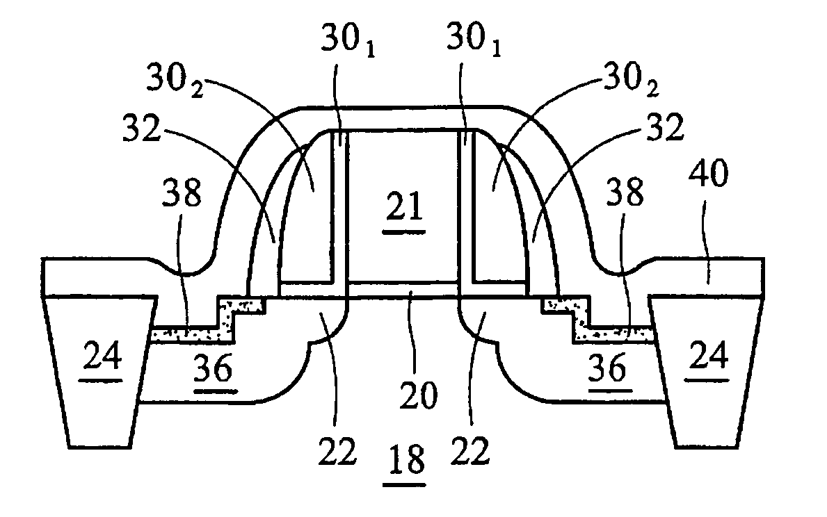
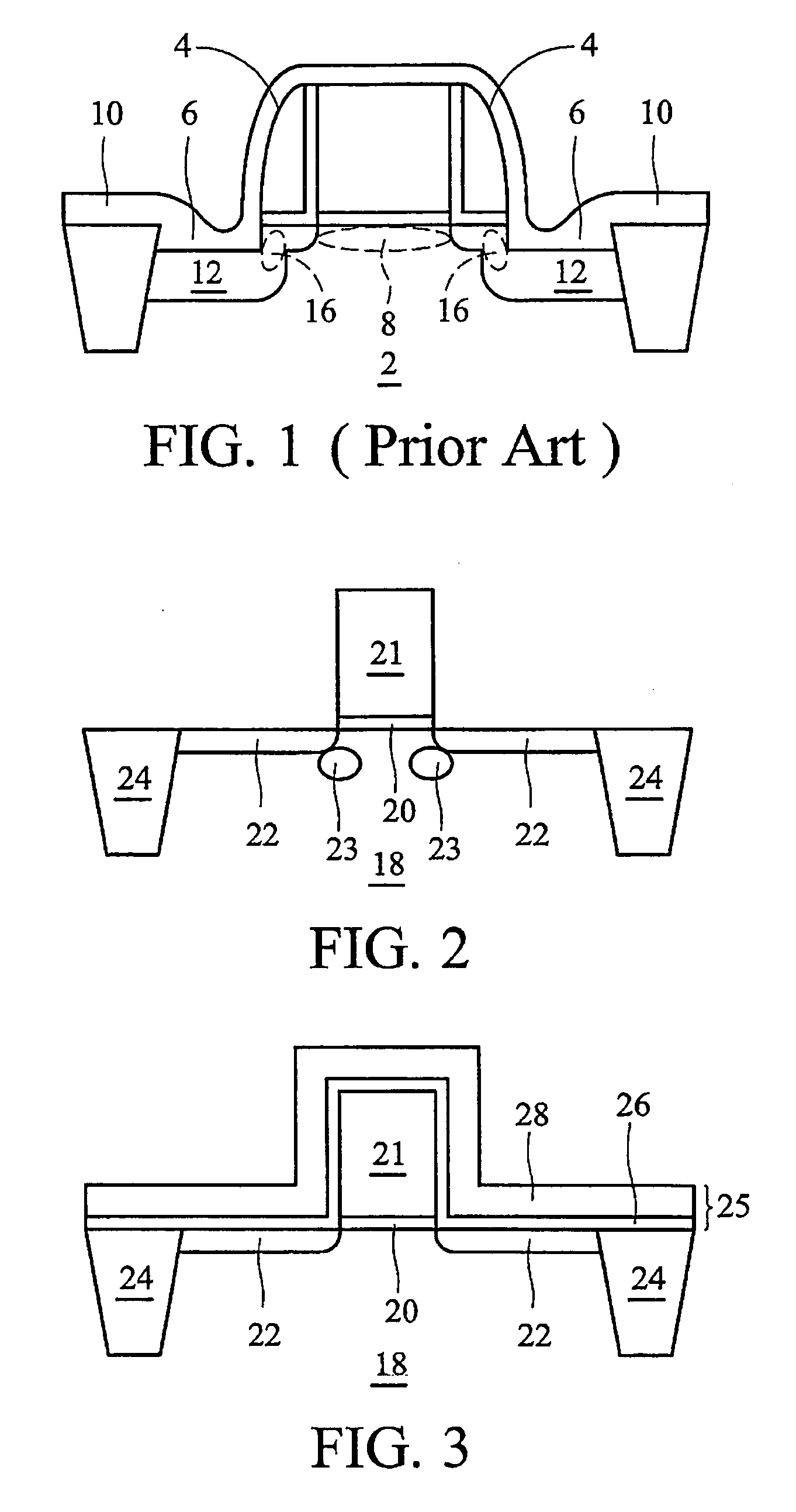
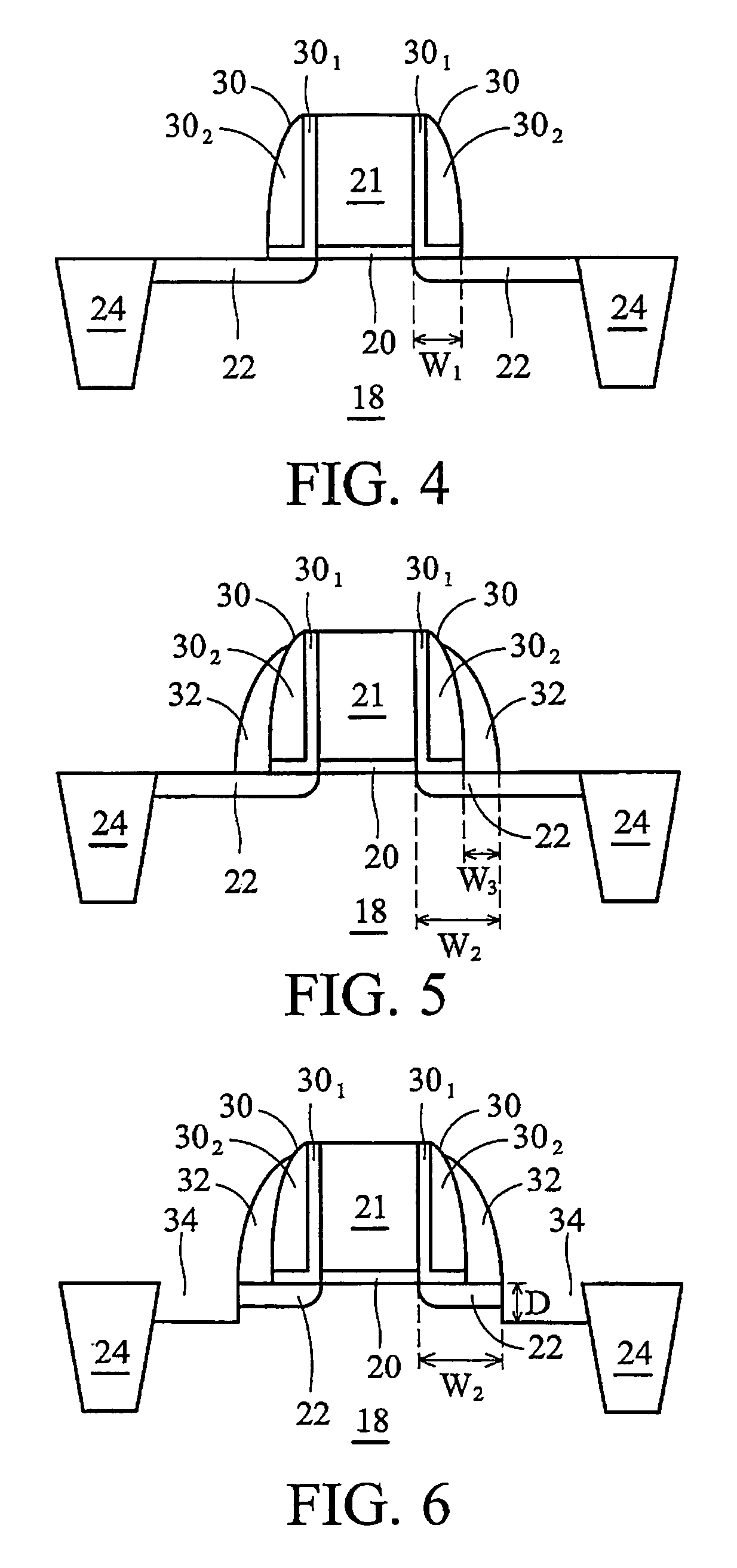
[0021]FIG. 2 illustrates the formation of a gate stack comprising a gate dielectric 20 and a gate electrode 21 on a substrate 18. The gate dielectric 20 preferably has high dielectric constant (k value). In the preferred embodiment, the substrate 18 comprises bulk silicon. In alternative embodiments, other commonly used materials and structures, such as germanium, SiGe, strained silicon on SiGe, silicon on insulator (SOI), silicon germanium on insulator (SGOI), germanium on insulator (GOI), and the like, can also be used. Shallow trench isolation regions (STI) 24 are formed i...


PUM


Abstract

A semiconductor device suffering fewer current crowding effects and a method of forming the same are provided. The semiconductor device includes a substrate, a gate over the substrate, a gate spacer along an edge of the gate and overlying a portion of the substrate, a diffusion region in the substrate wherein the diffusion region comprises a first portion and a second portion between the first portion and the gate spacer. The first portion of the diffusion region has a recessed top surface. The semiconductor device further includes a silicide layer on the diffusion region, and a cap layer over at least the silicide layer. The cap layer provides a strain to the channel region of the semiconductor device.

Description

TECHNICAL FIELD[0001]This invention generally relates to semiconductor devices and fabrication processes, and particularly to semiconductor device having a strained layer over source / drain regions.BACKGROUND[0002]The scaling of VLSI circuits is a constant effort. With circuits becoming smaller and faster, device drive current improvement becomes more important. Among efforts being made to improve device drive current, forming a strained silicon channel, thus enhancing carrier mobility, is a known practice. Strain, sometimes referred to as stress, can enhance bulk electron and hole mobility. The performance of a MOS device can be enhanced through a strained-surface channel. This technique allows performance to be improved at a constant gate length, without adding complexity to circuit fabrication or design.[0003]When silicon is placed under strain, the electron mobility is dramatically increased. One way to develop strain is by using a graded SiGe epitaxy layer as a substrate on whic...

Claims


Application Information

Patent Timeline
Patent Type & Authority Patents(United States)
IPC IPC(8): H01L29/772
CPCH01L29/41766H01L29/6659H01L29/66636H01L29/7843H01L29/456H01L29/6653H01L29/6656H01L29/7833Y10S257/90
Inventor WANG, CHIH-HAOWANG, TA-WEITSAI, CHING-WEI
Owner TAIWAN SEMICON MFG CO LTD
Why Eureka
Try Eureka