Buried dual taper waveguide for passive alignment and photonic integration

a taper waveguide and photonic integration technology, applied in the field of taper optical waveguides, can solve the problems of difficult to obtain good fiber-silicon waveguide coupling, large difference between the taper height and the final photonic waveguide height, and difficult to fabricate photonic components together with silicon taper

Inactive Publication Date: 2011-08-16
INTEL CORP
View PDF4 Cites 29 Cited by
  • Summary
  • Abstract
  • Description
  • Claims
  • Application Information

AI Technical Summary

Problems solved by technology

Due to the high refractive index contrast of silicon waveguide systems, obtaining good fiber-silicon waveguide coupling is very challenging particularly for small silicon rib waveguides.
This may result in a large difference between the taper height and final photonic waveguide height.
Such a topology on the silicon wafer may make it harder to fabricate photonic components together with silicon taper.

Method used


Image

  • Buried dual taper waveguide for passive alignment and photonic integration
  • Buried dual taper waveguide for passive alignment and photonic integration
  • Buried dual taper waveguide for passive alignment and photonic integration

Examples


Embodiment Construction

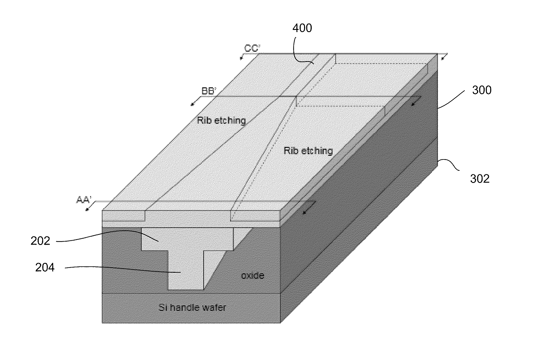
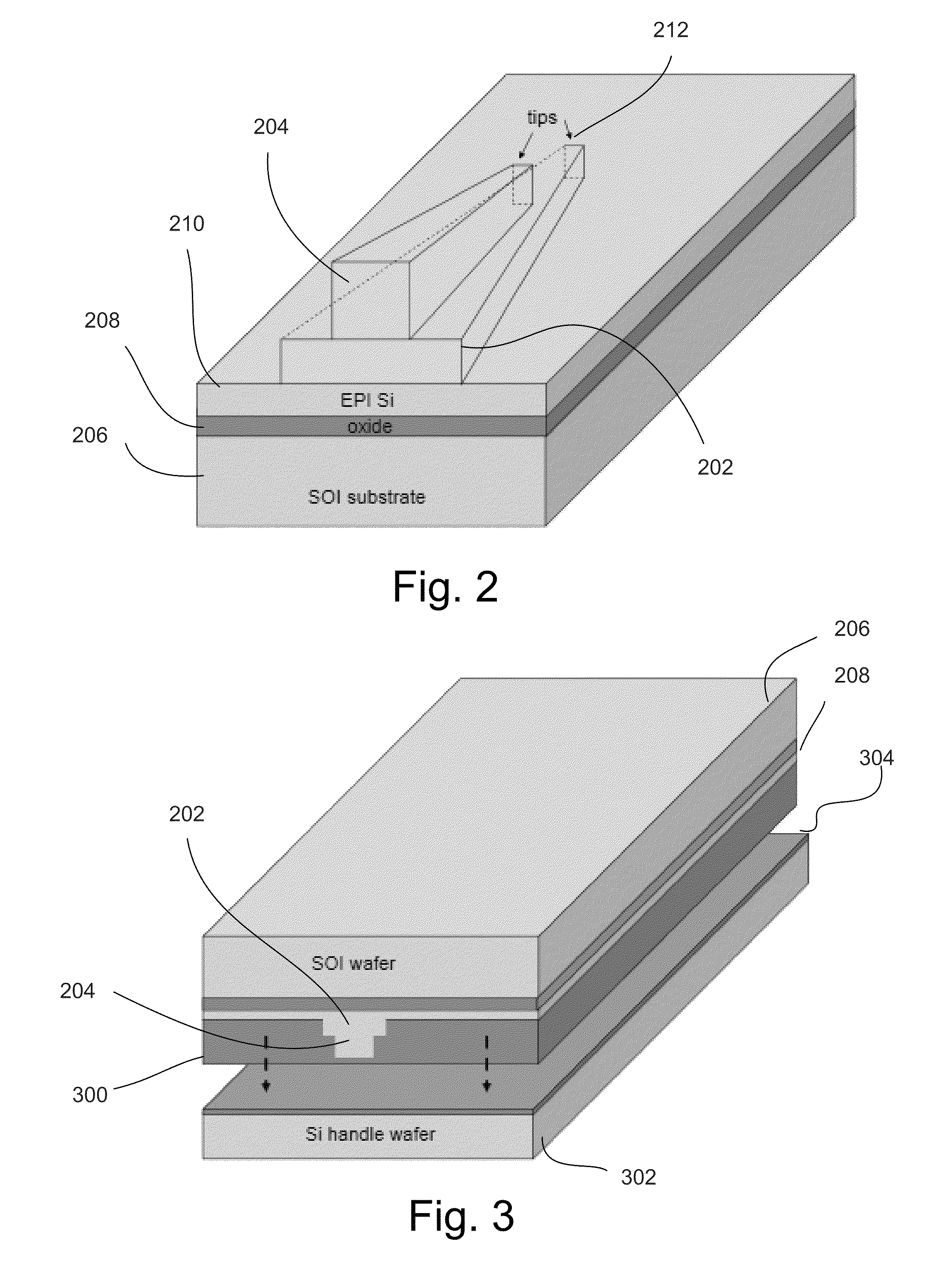
[0014]Described is a buried dual taper waveguide that has a flat surface after taper processing thus facilitating further processing with a more complex photonic integrated circuit. This allows for light coupling between a large core size fiber and a small waveguide photonic integrated circuit. The taper structure disclosed enables monolithic integration of silicon photonic components and passive alignment for low-cost packaging.

[0015]Reference throughout this specification to “one embodiment” or “an embodiment” means that a particular feature, structure, or characteristic described in connection with the embodiment is included in at least one embodiment of the present invention. Thus, the appearances of the phrases “in one embodiment” or “in an embodiment” in various places throughout this specification are not necessarily all referring to the same embodiment. Furthermore, the particular features, structures, or characteristics may be combined in any suitable manner in one or more ...


PUM


Abstract

A buried dual taper waveguide has a flat surface after taper processing thus facilitating further processing with more complex photonic integrated circuits. This allows for light coupling between a large core size fiber and a small waveguide photonic integrated circuit. The taper structure disclosed enables monolithic integration of silicon photonic components and passive alignment for low-cost packaging.

Description

FIELD OF THE INVENTION[0001]Embodiments of the present invention relate to waveguides, and more particularly, to tapered optical waveguides.BACKGROUND INFORMATION[0002]Efficient light coupling between an optical fiber and a silicon waveguide is highly desired for silicon based photonic device and circuit applications. Due to the high refractive index contrast of silicon waveguide systems, obtaining good fiber-silicon waveguide coupling is very challenging particularly for small silicon rib waveguides.[0003]Often is the case that an optical device includes a fiber or waveguide that is intended to be coupled to another waveguide having a significantly larger / smaller cross-sectional size. For example, a planar lightwave circuit (PLC) can have a waveguide on the order of four microns in height to be coupled to an optical fiber with a diameter of about ten microns. One way to couple a port of a relatively large waveguide to a port of a significantly smaller waveguide is by forming a tape...

Claims


Application Information

Patent Timeline
Patent Type & Authority Patents(United States)
IPC IPC(8): G02B6/12G02B6/10G02B6/34G02B6/32
CPCG02B6/12004G02B6/1228G02B6/124G02B6/305
Inventor LIU, ANSHENG
Owner INTEL CORP
Why Eureka
Try Eureka