Semiconductor wafer processing method that allows device regions to be selectively annealed following back end of the line (BEOL) metal wiring layer formation

a technology of semiconductor wafers and device regions, applied in the direction of semiconductor devices, electrical equipment, transistors, etc., can solve the problems of affecting performance and reducing the reliability of metal wiring

Inactive Publication Date: 2011-09-20
ULTRATECH INT INC
View PDF26 Cites 18 Cited by
  • Summary
  • Abstract
  • Description
  • Claims
  • Application Information

AI Technical Summary

Benefits of technology

[0006]One exemplary embodiment of the method can comprise providing a wafer that has a bottom surface and a top surface opposite the bottom surface. A semiconductor device and, particularly, a field effect transistor can be formed adjacent to the top surface. The process of forming the semiconductor device can comprising forming a gate structure on a channel region such that the gate structure comprises a gate dielectric layer adjacent to the channel region, a gate conductor layer adjacent to the gate dielectric layer and an infrared absorbing layer positioned either between the gate dielectric layer and the gate conductor layer or above the gate conductor layer. The infrared absorbing layer can comprise, for example, a doped germanium layer. Then, BEOL processing can be performed. That is, at least one dielectric layer can be formed on the semiconductor device and at least one layer of metal wiring can be formed on the dielectric layer. Following BEOL metal wiring layer formation, the infrared absorbing layer within the gate structure can be selectively heated to a first predetermined temperature (e.g., a dopant activation temperature, a temperature required for a state change, etc.) by exposing the bottom surface of the wafer to an infrared light having a wavelength that is transparent to the wafer, but absorbed by the infrared absorbing layer. This selective heating process can be performed so that heat from the infrared absorbing layer is transferred to the channel region below the gate structure and, optionally, to one or more additional regions of the device adjacent to the channel region (e.g., source / drain regions, halos, and / or source / drain extensions) without raising the temperature of the metal wiring above a second predetermined temperature (e.g., a temperature that could degrade the metal wiring, such as the melting temperature of the metal wiring material) that is lower than the first predetermined temperature.

Problems solved by technology

It would be advantageous to be able to perform a thermal anneal following back end of the line (BEOL) metal wiring layer formation; however, the temperature and processing time typically required for such thermal anneals can degrade the reliability of the metal wiring and, thereby impact performance.

Method used


Image

  • Semiconductor wafer processing method that allows device regions to be selectively annealed following back end of the line (BEOL) metal wiring layer formation
  • Semiconductor wafer processing method that allows device regions to be selectively annealed following back end of the line (BEOL) metal wiring layer formation
  • Semiconductor wafer processing method that allows device regions to be selectively annealed following back end of the line (BEOL) metal wiring layer formation

Examples


Embodiment Construction

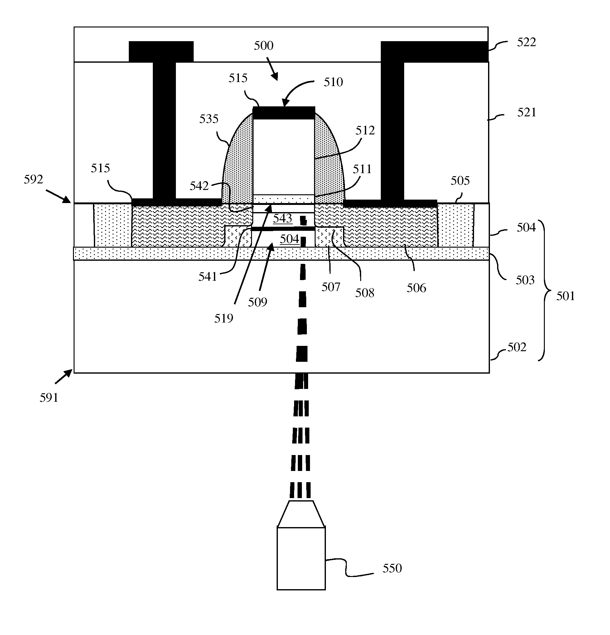
[0024]The embodiments of the invention and the various features and advantageous details thereof are explained more fully with reference to the non-limiting embodiments that are illustrated in the accompanying drawings and detailed in the following description.

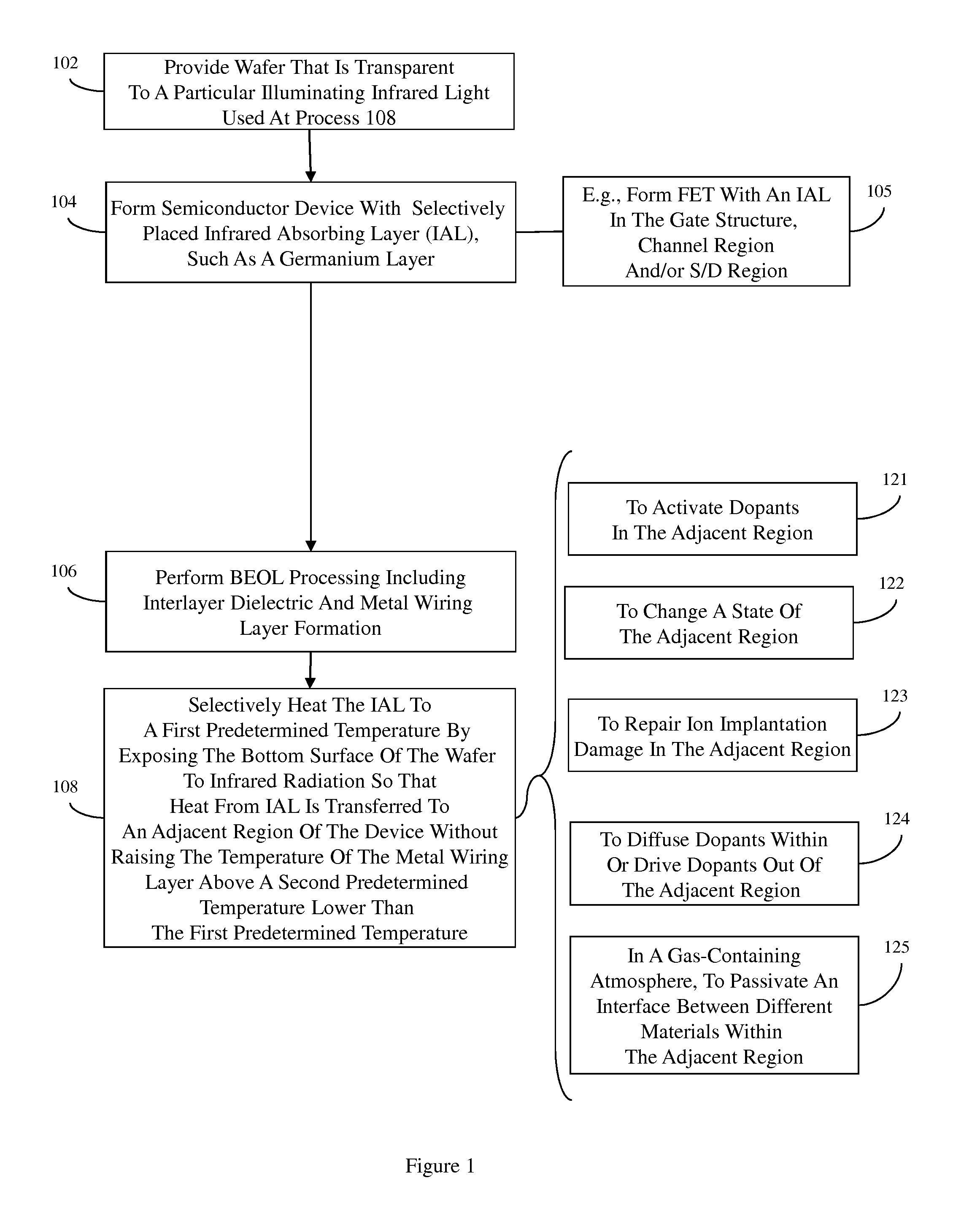
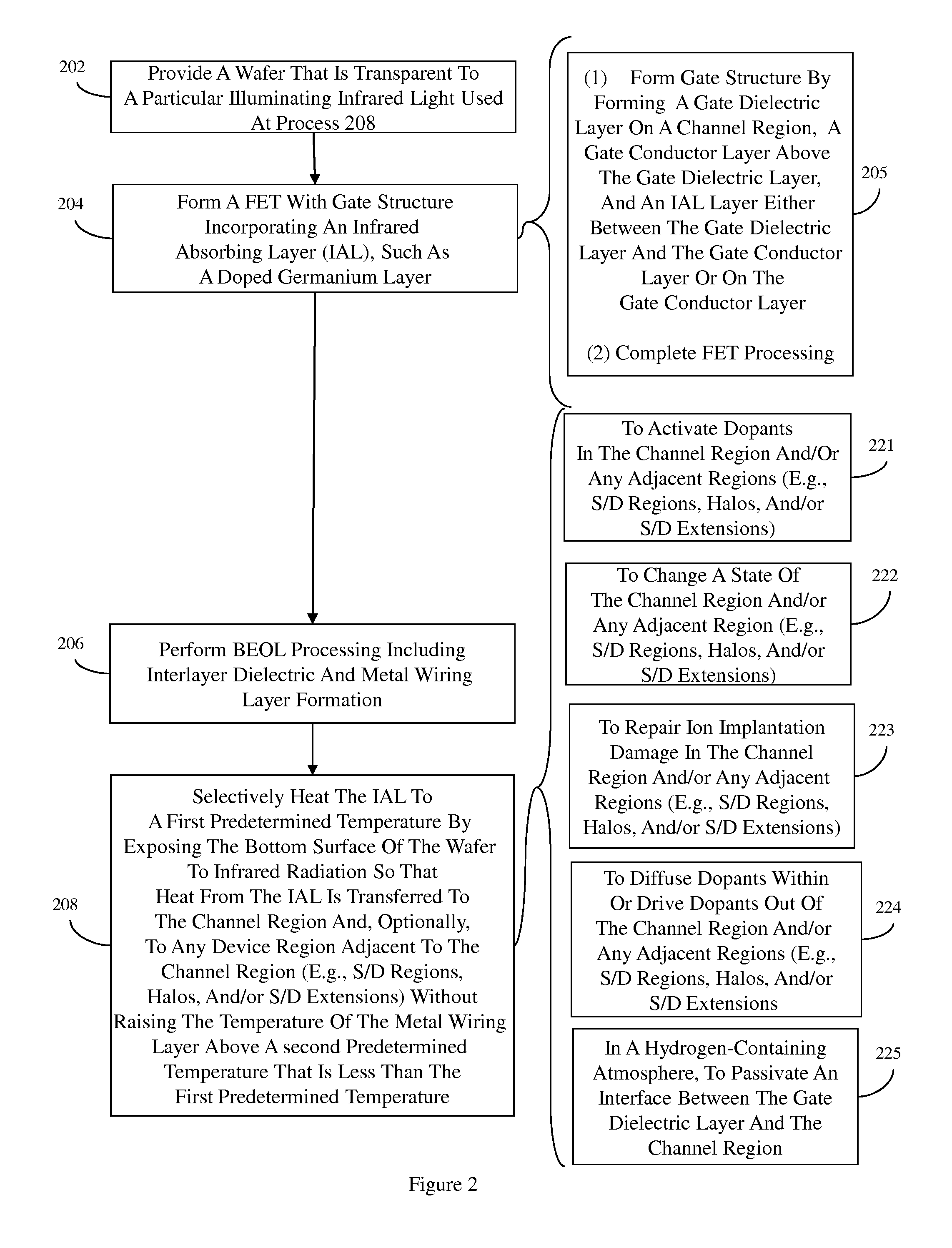
[0025]As mentioned above, thermal anneals are often performed during middle of the line (MOL) semiconductor wafer processing in order to repair damage caused by the implantation of dopants (e.g., source / drain dopants), to diffuse or drive dopants, to activate those dopants, to change the state of semiconductor material (e.g., to crystallize or recrystallize semiconductor material), etc. Thermal anneals can also be used to passivate an interface between different materials (e.g., an interface between a semiconductor layer and a dielectric layer), when performed in the presence of a gas, such as hydrogen. It would be advantageous to be able to perform a thermal anneal following back end of the line (BEOL) metal wiring layer form...


PUM


Abstract

Disclosed are embodiments of a semiconductor wafer processing method that allow device regions to be selectively annealed following back end of the line (BEOL) metal wiring formation without degrading wiring layer reliability. In the embodiments, a semiconductor device is formed adjacent to the top surface of a wafer such that it incorporates a selectively placed infrared absorbing layer (IAL). Then, following BEOL metal wiring formation, the bottom surface of the wafer is exposed to an infrared light having a wavelength that is transparent to the wafer. The infrared light is absorbed by and, thereby heats up the IAL to a first predetermined temperature (e.g., a dopant activation temperature, a temperature required for a state change, etc.). The resulting heat is transferred from the IAL to an adjacent region of the semiconductor device without raising the temperature of the metal wiring above a second predetermined temperature (e.g., a temperature that could degrade the metal wiring) that is lower than the first predetermined temperature.

Description

BACKGROUND[0001]1. Field of the Invention[0002]The present invention relates to semiconductor wafer processing and, more specifically, to embodiments of a semiconductor wafer processing method that allow device regions to be selectively annealed following back end of the line (BEOL) metal wiring layer formation.[0003]2. Description of the Related Art[0004]Thermal anneals are often performed during middle of the line (MOL) semiconductor wafer processing in order to repair damage caused by the implantation of dopants (e.g., source / drain dopants), to diffuse dopants, to activate those dopants, to change the state of semiconductor material (e.g., to crystallize or recrystallize semiconductor material), etc. Thermal anneals can also be used to passivate an interface between different materials (e.g., an interface between a semiconductor layer and a dielectric layer) when performed in the presence of a gas, such as hydrogen. It would be advantageous to be able to perform a thermal anneal ...

Claims


Application Information

Patent Timeline
Patent Type & Authority Patents(United States)
IPC IPC(8): H01L21/336
CPCH01L21/268H01L21/28044H01L29/1054H01L29/4925H01L29/665H01L29/7833H01L29/6659
Inventor ABADEER, WAGDI W.KAMAL, LEGAL REPRESENTATIVE, LILIANELLIS-MONAGHAN, JOHN J.GAMBINO, JEFFREY P.LEE, TOM C.
Owner ULTRATECH INT INC
Why Eureka
Try Eureka