Semiconductor device

a technology of semiconductors and devices, applied in the field of semiconductor devices, can solve the problems of difficult to determine the writing condition for obtaining the desired resistance value by the rewrite operation, and achieve the effect of facilitating multi-bit operation

Active Publication Date: 2006-06-15
RENESAS ELECTRONICS CORP
View PDF8 Cites 82 Cited by
  • Summary
  • Abstract
  • Description
  • Claims
  • Application Information

AI Technical Summary

Benefits of technology

[0009] Therefore, an object of the present invention to provide a technology capable of suppressing a variation in a value a...

Problems solved by technology

Since the write operation is influenced by the resistance value before the write operation, it is very ...

Method used


Image

  • Semiconductor device
  • Semiconductor device
  • Semiconductor device

Examples


Embodiment Construction

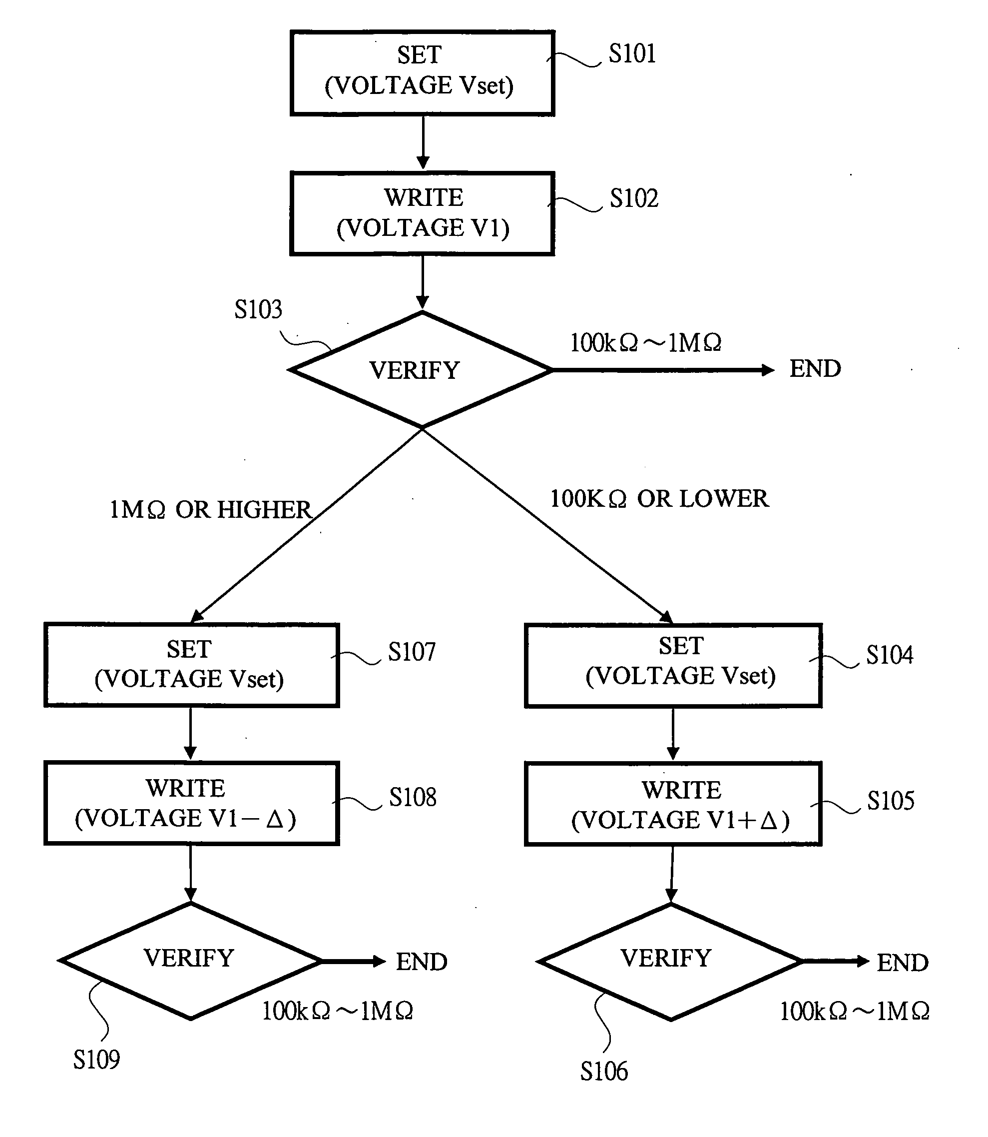
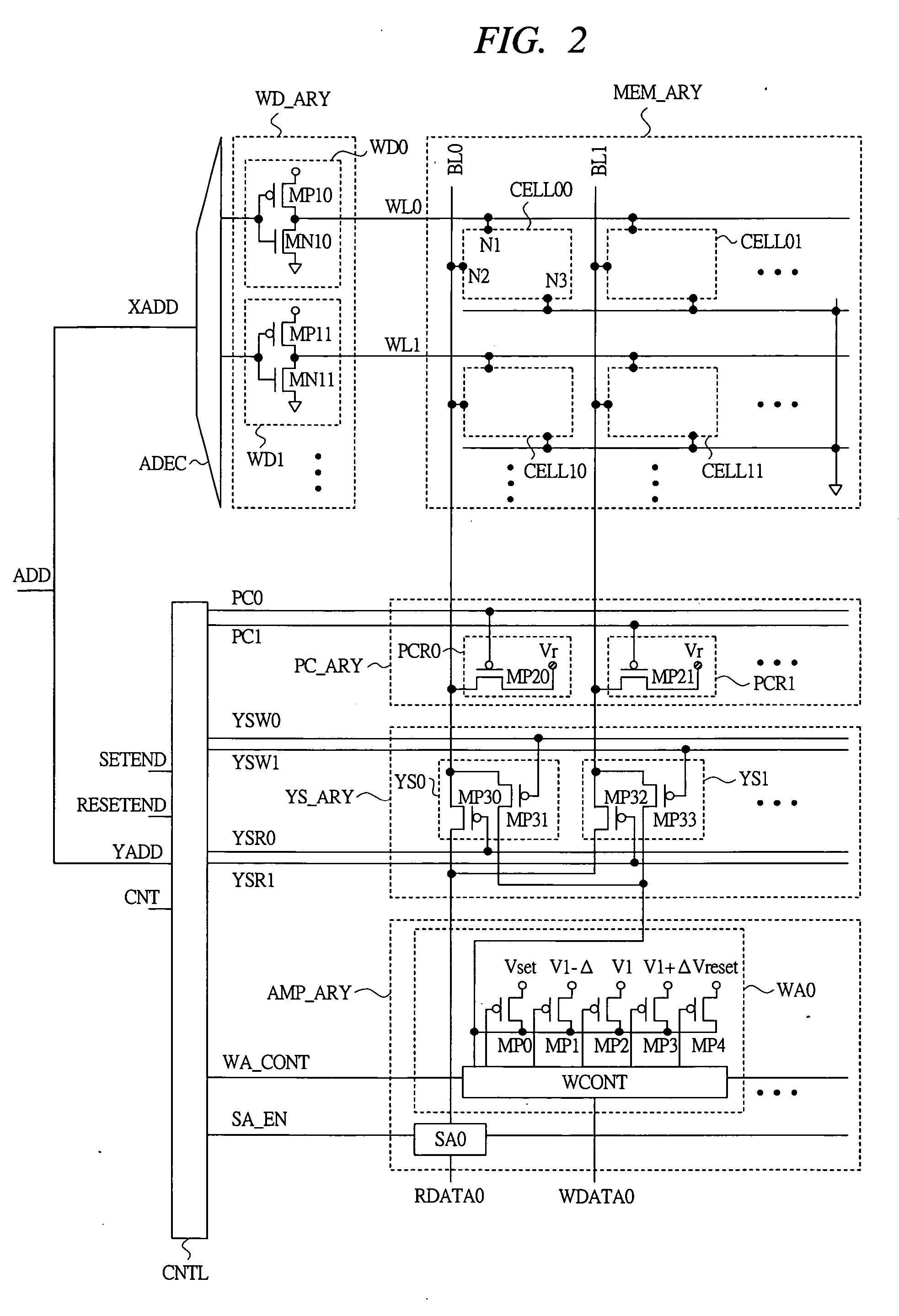
[0030] Hereinafter, embodiments of the present invention will be described in detail with reference to the accompanying drawings. Note that components having the same function are denoted by the same reference symbols throughout the drawings for describing the embodiment, and the repetitive description thereof will be omitted. A symbol representing the name of a terminal is used also as a name of a wiring and a signal, and a symbol representing the name of a power supply is used also as a voltage value thereof unless otherwise specified.

[0031] Circuit components which compose respective function blocks in the embodiments are not particularly limited, but are formed on one semiconductor substrate such as that made of single crystal silicon by a publicly-known semiconductor integrated circuit technology such as CMOS (complementary MOS transistor). In the drawings, the connection of substrate potentials of the MOS transistors is not particularly shown, but a connecting method is not p...


PUM


Abstract

The present invention provides a technology which can suppress a variation in a value after a write operation to minimum so as to facilitate multi-bit operation in a semiconductor device such as a phase change memory. A semiconductor device includes: a memory cell having a storage element (phase change material) that stores information depending on a state change by temperature; an I/O circuit; and means which, when writing data, performs a set operation and an operation for writing desired data, measures a resistance value of the storage element by means of a verify operation, and when the resistance value is not within a target range, performs the set operation and the write operation again while changing a voltage to be applied to the storage element.

Description

CROSS-REFERENCE TO RELATED APPLICATION [0001] The present application claims priority from Japanese Patent Application No. JP 2004-341475 filed on Nov. 26, 2004, the content of which is hereby incorporated by reference into this application. TECHNICAL FIELD OF THE INVENTION [0002] The present invention relates to a semiconductor device. More particularly, it relates to an on-chip memory, which is mounted on a non-volatile memory and a system LSI (microcomputer and the like). BACKGROUND OF THE INVENTION [0003] As a technology in the field of the non-volatile memories and on-chip memories examined by the inventors of the present invention, for example, the following technologies are known. [0004] In order to attain high-speed and highly-integrated non-volatile memories, phase change memories are being developed. The phase change memories are disclosed in Japanese Patent Application Laid-Open Publication No. 2003-100084 (Patent Document 1), the specification of U.S. Pat. No. 6,625,054 ...

Claims


Application Information

Patent Timeline
IPC IPC(8): G11C11/00
CPCG11C11/5678G11C13/0004G11C13/003G11C13/0064G11C13/0069G11C2013/009G11C2013/0092G11C2213/74G11C2213/79G11C13/0061
Inventor OSADA, KENICHIKAWAHARA, TAKAYUKI
Owner RENESAS ELECTRONICS CORP
Why Eureka
Try Eureka