Solid-state imaging device with an organic photoelectric conversion film and imaging apparatus

a technology of organic photoelectric conversion film and imaging device, which is applied in the direction of radiological control devices, instruments, television systems, etc., can solve the problems of poor color reproducibility and difficulty in applying the device to a general high-resolution image sensor, and achieve excellent color reproducibility and excellent color reproducibility. , the effect of improving the quality of taken images

Active Publication Date: 2011-10-11
SONY SEMICON SOLUTIONS CORP
View PDF10 Cites 49 Cited by
  • Summary
  • Abstract
  • Description
  • Claims
  • Application Information

AI Technical Summary

Benefits of technology

[0011]It is desirable to improve the color reproducibility so that a device can be applied to a high-resolution image sensor.
[0013]In the solid-state imaging device according to the embodiment of the present invention, since the number of organic-photoelectric-conversion films is one, the problem of the harmonization between a process for lead electrodes, which are normally metal films, and a process for the organic-photoelectric-conversion film can be avoided. Additionally, by disposing elements corresponding to the plurality of colors not including the first color, for example, as a checker pattern, in the organic-color-filter layer, the color reproducibility can be markedly improved.
[0015]In the imaging apparatus according to the embodiment of the present invention, the solid-state imaging device according to the embodiment of the present invention, i.e., a solid-state imaging device having an excellent color reproducibility, is used.
[0016]Therefore, an imaging apparatus with an excellent color reproducibility can be provided by including the solid-state imaging device according to the embodiment of the present invention. The solid-state imaging device has an advantage in that the problem of the harmonization between a process for the organic-photoelectric-conversion film and a process for lead electrodes, which are normally metal films, can be avoided.
[0017]In the imaging apparatus according to the embodiment of the present invention, since that solid-state imaging device having an excellent color reproducibility can be used in the imaging apparatus, the quality of taken images can be improved. Accordingly, the imaging apparatus has an advantage in that high-quality images can be recoded.

Problems solved by technology

In a device in the related art, when the difference of absorption of light with different wavelengths in a bulk of silicon is utilized, the color reproducibility is poor.
For this reason, it is difficult to apply the device to a general high-resolution image sensor.

Method used


Image

  • Solid-state imaging device with an organic photoelectric conversion film and imaging apparatus
  • Solid-state imaging device with an organic photoelectric conversion film and imaging apparatus
  • Solid-state imaging device with an organic photoelectric conversion film and imaging apparatus

Examples


Embodiment Construction

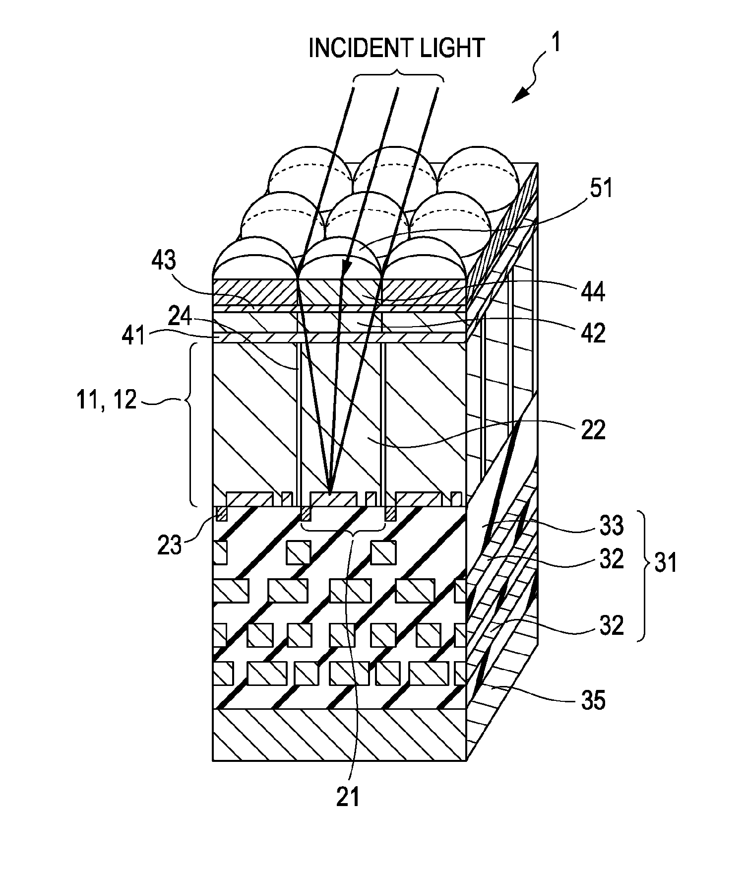
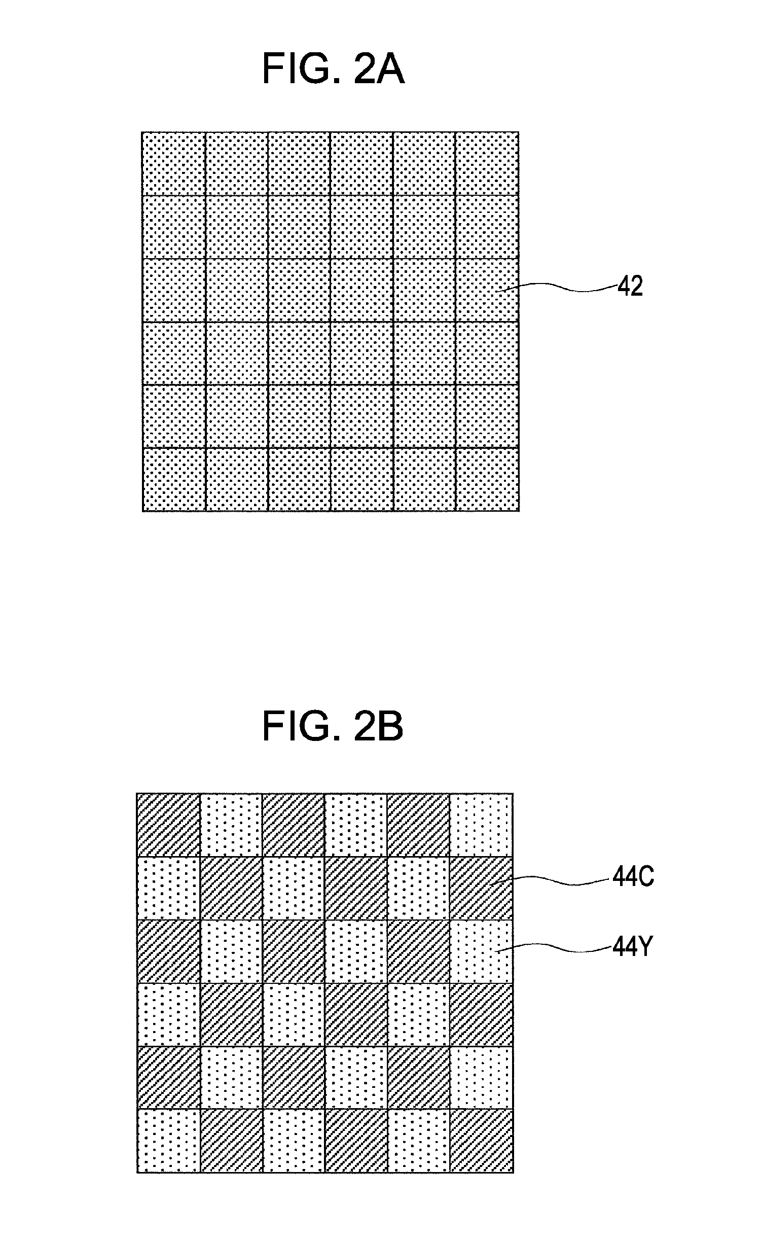
[0025]A solid-state imaging device according to an embodiment (a first embodiment) of the present invention will be described with reference to a schematic perspective view of a configuration thereof shown in FIG. 1 and layout diagrams shown in FIGS. 2A and 2B. Referring to FIG. 1, a whole-area-open-type CMOS image sensor is shown as an application example of the solid-state imaging device according to the first embodiment of the present invention.

[0026]As shown in FIG. 1, in an active layer 12, which is formed of a semiconductor substrate 11, pixel units 21 including photoelectric-conversion units (for example, photodiodes) 22, each of which converts incident light to an electric signal, and a group of transistors 23 having transfer transistors, amplifying transistors, reset transistors, or the like (a portion of the group of transistors 23 shown in FIG. 1) are formed. As the semiconductor substrate 11, for example, a silicon substrate can be used. Additionally, a signal-processing...


PUM


Abstract

There is provided a solid-state imaging device including a plurality of pixels that are provided on a semiconductor substrate, and that include a plurality of photoelectric-conversion units and metal oxide semiconductor transistors that selectively read signals from the plurality of photoelectric-conversion units, an organic-photoelectric-conversion film disposed on the plurality of photoelectric-conversion units, and an organic-color-filter layer disposed on the plurality of photoelectric-conversion units. Only a signal corresponding to a first color is extracted through the organic-photoelectric-conversion film. Signals corresponding to a plurality of colors not including the first color are extracted by absorption spectroscopy using the organic-color-filter layer.

Description

CROSS REFERENCES TO RELATED APPLICATIONS[0001]The present invention contains subject matter related to Japanese Patent Application JP 2007-100266 filed in the Japanese Patent Office on Apr. 6, 2007, the entire contents of which are incorporated herein by reference.BACKGROUND OF THE INVENTION[0002]1. Field of the Invention[0003]The present invention relates to solid-state imaging devices and imaging apparatuses.[0004]2. Description of the Related Art[0005]Semiconductor image sensors, which are solid-state imaging devices, include complementary metal-oxide semiconductor (CMOS) sensors and charge-coupled devices (CCDs). The CMOS sensors include a plurality of pixels, which have photoelectric-conversion units that convert incident light to electric signals, and metal-oxide semiconductor (MOS) transistors that selectively read the electric signals from each of the pixels. The CCDs include a plurality of pixels, which have photoelectric-conversion units that convert incident light to elec...

Claims


Application Information

Patent Timeline
Patent Type & Authority Patents(United States)
IPC IPC(8): H04N3/14H04N9/04H01L27/00H01L31/062H01L27/14H01L27/146H04N9/07
CPCH01L27/14621H01L27/14627H01L27/307H01L27/302H04N9/045H04N25/13H04N25/17H01L27/146H04N23/12
Inventor TAKIZAWA, RITSUONATORI, TAICHI
Owner SONY SEMICON SOLUTIONS CORP
Why Eureka
Try Eureka