Semiconductor device

a technology of semiconductor devices and semiconductors, applied in semiconductor devices, semiconductor/solid-state device details, electrical apparatus, etc., can solve the problems of disturbed high-density formation of above-described conductive members, difficulty in sufficiently filling the spacing between the chips with underfill resin, and affecting the connection density between the chips. , to achieve the effect of improving electrical characteristics and reducing electric resistance through the signal path

Inactive Publication Date: 2011-10-18
RENESAS ELECTRONICS CORP
View PDF13 Cites 4 Cited by
  • Summary
  • Abstract
  • Description
  • Claims
  • Application Information

AI Technical Summary

Benefits of technology

[0010]On the contrary, according to the semiconductor device of the non-patent document 1, a spacing between the first and the second semiconductor chips is air-tightly sealed with a seal ring, so that a certain connection reliability between both chips can be maintained for longer term, without a need for filling the spacing with an underfill resin. Therefore, it is preferable to provide a seal ring between the first and the second semiconductor chips, in view of improving a connection density between both chips.
[0013]In this semiconductor device, the region (internal region) that is surrounded by the seal ring and the region (external region) that is not surrounded by the seal ring are provided between the first and the second semiconductor chips. This configuration achieves that both chips can be electrically connected in the external region, in addition to in the internal region. Therefore, by utilizing such external region, a signal of one of the chips can be picked up without transferring the signal through an internal interconnect of the other chip. Consequently, a reduced electric resistance through the signal path can be provided.
[0014]According to the present invention, the semiconductor device exhibiting improved electrical characteristics can be achieved.

Problems solved by technology

However, when too much smaller spacing is provided between the conductive members such as a bump for connecting both chips, it becomes difficult to sufficiently fill the spacing between the chips with the underfill resin.
This disturbs a high-density formation of the above-described conductive members.
In other words, an improvement in the connection density between both chips is disturbed.
Accordingly, an electric resistance through the signal path is increased, leading to a deterioration of electrical characteristics of the semiconductor device.

Method used


Image

  • Semiconductor device
  • Semiconductor device
  • Semiconductor device

Examples


first embodiment

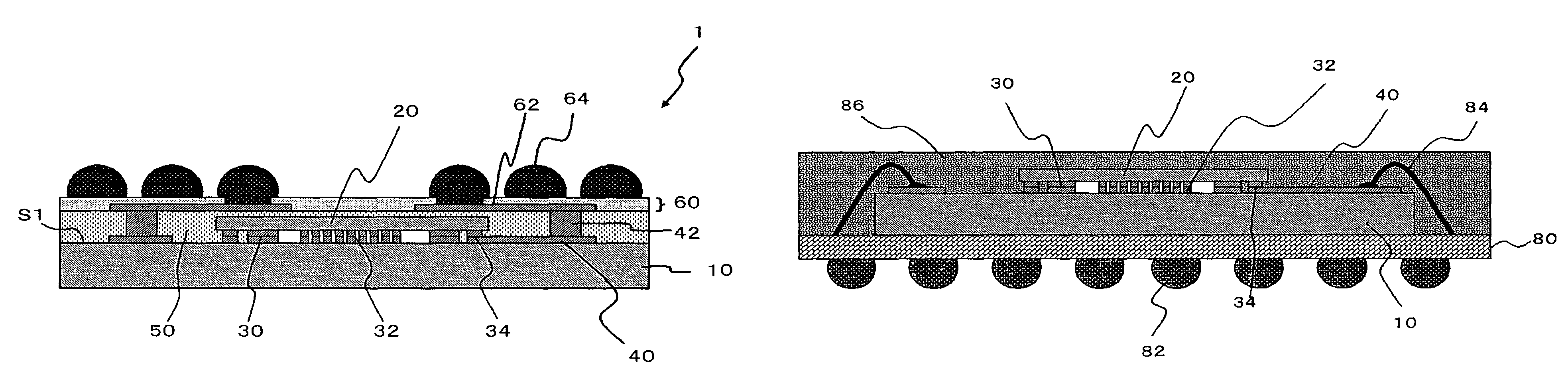
[0026]FIG. 1 is a cross-sectional view of a semiconductor device, illustrating a configuration of a semiconductor device of the first embodiment according to the present invention. A semiconductor device 1 includes a semiconductor chip 10 (first semiconductor chip), a semiconductor chip 20 (second semiconductor chip) and a seal ring 30.

[0027]The semiconductor chip 20 is provided on the surface S1 of the semiconductor chip 10 so as to be spaced apart from the semiconductor chip 10 with a predetermined spacing therebetween. In the present embodiment, the semiconductor chip 10 has a larger chip area than the semiconductor chip 20 has. The semiconductor chip 10 and semiconductor chip 20 are, for example, a memory chip and a logic LSI chip, respectively.

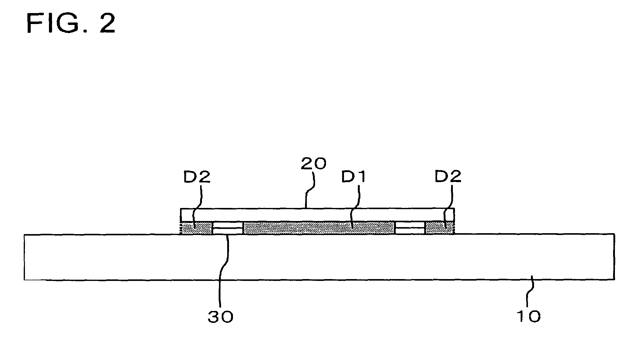
[0028]A seal ring 30 is interposed between the semiconductor chip 10 and the semiconductor chip 20. More specifically, the semiconductor chip 20 is disposed on the semiconductor chip 10 via the seal ring 30. As shown in FIG. 2, an interna...

second embodiment

[0048]FIG. 6 is a cross-sectional view, illustrating the second embodiment of a semiconductor device according to the present invention. In the semiconductor device 2, a portion of the interconnect 40 is provided on the surface S1 of the semiconductor chip 10 through the insulating film 70. That is, the insulating film 70 is formed on the semiconductor chip 10, and a portion of the interconnect 40 is formed thereon. More specifically, a portion of the interconnect 40, which is connected to the conductive member 34, is formed directly on the semiconductor chip 10, and meanwhile, a portion thereof connected to the conductor post 42 is formed on the insulating film 70. It is preferable that the insulating film 70 is an organic insulating film. Other configurations of the semiconductor device 2 are similar to those of the semiconductor device 1.

[0049]The semiconductor device 2 having such configurations can exhibit the following advantageous effect, in addition to the advantageous effec...


PUM


Abstract

A semiconductor device 1 includes a semiconductor chip 10 (first semiconductor chip), a semiconductor chip 20 (second semiconductor chip) and a seal ring 30. The semiconductor chip 20 is provided on a surface S1 of the semiconductor chip 10 so as to be spaced apart from the semiconductor chip 10 with a predetermined spacing therebetween. A seal ring 30 is interposed between the semiconductor chip 10 and the semiconductor chip 20. An internal region, which is an inner region of the seal ring 30, and an external region, which is an outer region of the seal ring 30, are provided between the semiconductor chip 10 and the semiconductor chip 20.

Description

[0001]This application is based on Japanese patent application No. 2005-294710, the content of which is incorporated hereinto by reference.BACKGROUND[0002]1. Technical Field[0003]The present invention relates to a semiconductor device.[0004]2. Related Art[0005]Conventional semiconductor devices include those disclosed in the patent document 1 and the non-patent document 1, cited below. In the semiconductor device described in the patent document 1, a second semiconductor chip is flip-chip mounted on a first semiconductor chip. A gap between the first and the second semiconductor chips is filled with an underfill resin.[0006](Patent document 1) Japanese Laid-open patent publication No. 2003-17654[0007](Non-patent document 1) Bernard Levine, “SYSTEM-IN-PACKAGE: Growing Markets, Ongoing Uncertainty”, SEMICONDUCTOR MANUFACTURING, March 2004, pp. 47 to 61[0008]Meanwhile, in the semiconductor device described in the non-patent document 1, a second semiconductor chip is disposed on a first...

Claims


Application Information

Patent Timeline
Patent Type & Authority Patents(United States)
IPC IPC(8): H01L23/52
CPCH01L23/3114H01L25/0657H01L25/18H01L2224/48091H01L2224/48227H01L2225/06513H01L2924/12044H01L2924/00014H01L24/48H01L2924/181H01L2924/00012H01L2224/45099H01L2224/45015H01L2924/207
Inventor KURITA, YOICHIRO
Owner RENESAS ELECTRONICS CORP
Why Eureka
Try Eureka