Watertight circuit board fabrication method

A manufacturing method and circuit board technology, applied in the electronic field, can solve the problems of large occupied area of ​​chips and devices, signal delay, large power consumption, etc., and achieve the effect of increasing connection density, avoiding position movement, and avoiding displacement

Inactive Publication Date: 2019-02-15
SHENZHEN XIUYI INVESTMENT DEV PARTNERSHIP LLP
View PDF2 Cites 0 Cited by
  • Summary
  • Abstract
  • Description
  • Claims
  • Application Information

AI Technical Summary

Problems solved by technology

[0002] At present, in the semiconductor packaging and patching process, surface mount, flip soldering, ball grid array, wire bonding and other packaging processes are usually used. The chip and device occupy a large area and have a high thickness, so that the packaged device has a large area and a large thickness, and This traditional packaging process makes the internal interconnection wires of the package body longer, resulting in high power consumption and signal delay, which cannot meet the needs of UHF circuits.

Method used


Image

  • Watertight circuit board fabrication method
  • Watertight circuit board fabrication method
  • Watertight circuit board fabrication method

Examples


Embodiment 1

[0080] Such as Figures 1 to 8 Shown is a step diagram of the method for making the watertight circuit board in this embodiment.

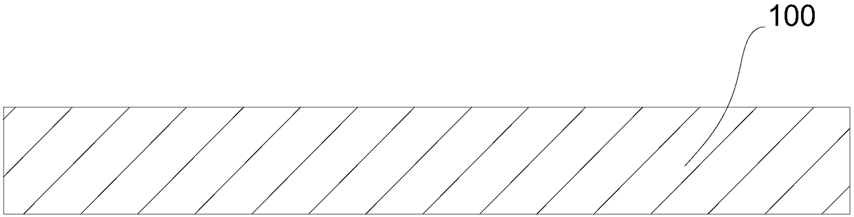
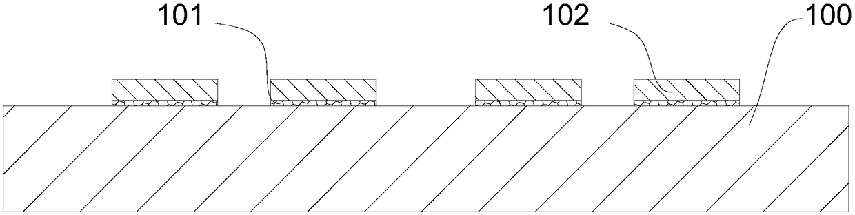
[0081] This is the example, such as figure 1 As shown, the sealing base layer 100 is a whole made of glass plate, and the sealing base layer 100 is made by processing a glass plate whose thickness, size, and physical / chemical / mechanical properties meet the requirements. Such as figure 2 As shown, the electronic component 102 with component pins is pasted on the sealing base layer 100 with a patch material 101 (which can be liquid, solid or film), and the position of the electronic component 102 on the sealing base layer is fixed to avoid electronic components in the subsequent process. Part 102 is displaced, affecting the connection. In this embodiment, the electronic component 102 is a chip with chip pins, and the chip pins are component pins (but not limited thereto, and may also be bare chips, electronic components, electronic devices, or ot...

Embodiment 2

[0091] The difference between embodiment two and embodiment one is:

[0092] Such as Figure 9 , 10 As shown, the sealing substrate has its own patch groove 110, or the patch groove 110 is made on the upper surface of the sealing base layer 100 by photolithography, wet etching, dry etching or other processes, such as Figure 11 As shown, the electronic component 102 is pasted in the patch groove 110 through the patch material 101 . The position of the electronic component 102 is limited by the patch groove 110 to avoid displacement of the electronic component 102 in subsequent processes.

[0093] Wherein, the sealing base layer 100 is a whole, and the whole itself has patch grooves 110 ; or, the sealing base layer 100 is a multi-layer structure, and the uppermost layer has patch grooves 110 .

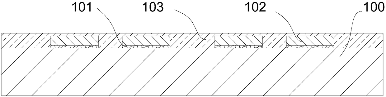
[0094] Such as Figure 12 As shown, the sealing base layer 100 is covered with a first insulating layer 103 , and the first insulating layer 103 and the sealing base layer 100 encap...

Embodiment 3

[0102] The difference between embodiment three and embodiment one is:

[0103] Such as Figure 19 , 20 As shown, the first insulating layer 103 is a two-layer laminated structure, including a first insulating layer 103A and a second insulating layer 103 . Such as Figure 20 As shown, the first via hole 104 passes through the first first insulating layer 103A and the second first insulating layer 103B.

[0104] The material, thickness, and area covered on the watertight substrate can be selected according to needs, and the first first insulating layer 103A and the second first insulating layer 103 can use the same or different materials. In this embodiment, the first insulating layer 103 has a stacked structure of two layers, but it is not limited thereto, and a stacked structure of more than three layers may also be used. Similarly, the second insulating layer 106 may also adopt a multi-layer structure similar to that of the first insulating layer 103 .


PUM


Abstract

The invention relates to and provides a watertight circuit board fabrication method. The watertight circuit board fabrication method comprises the steps of arranging an electronic part with a part pinon a sealing base layer; covering the sealing base layer with a first insulation layer, wherein the first insulation layer and the sealing base layer are used for encapsulating the electronic part; forming a first communication hole in the first insulation layer, wherein the first communication hole is corresponding to a position of the part pin of the electronic part; arranging a wiring layer onthe first insulation layer, wherein the wiring layer is electrically connected with the part pin by the first communication hole; and arranging a second insulation layer on the wiring layer, whereinthe second insulation layer and the first insulation layer are used for encapsulating the wiring layer, and first insulation layer and/or the second insulation layer are/is watertight materials. Withthe adoption of simple process steps, watertight package is achieved, and meanwhile, the thickness, the volume and the power consumption of a package body can be reduced.

Description

technical field [0001] The invention belongs to the field of electronics, and in particular relates to a method for manufacturing a watertight circuit board. Background technique [0002] At present, in the semiconductor packaging and patching process, surface mount, flip soldering, ball grid array, wire bonding and other packaging processes are usually used. The chip and device occupy a large area and have a high thickness, so that the packaged device has a large area and a large thickness, and This traditional packaging process makes the internal interconnection wires of the package body longer, resulting in high power consumption and signal delay, which cannot meet the needs of ultra-high frequency circuits. Contents of the invention [0003] Based on this, the present invention overcomes the defects of the prior art and provides a method for manufacturing a watertight circuit board, which can reduce the thickness, volume and power consumption of the package while imple...

Claims


Application Information

Patent Timeline
Patent Type & Authority Applications(China)
IPC IPC(8): H01L21/50H01L21/52H01L21/56
CPCH01L21/50H01L21/52H01L21/561H01L2224/18H01L2224/73267H01L2224/04105H01L2224/12105H01L2924/15153H01L2224/32225H01L2224/92244H01L24/19H01L24/20H01L2223/6677
Inventor 胡川燕英强郭跃进皮迎军刘俊军
Owner SHENZHEN XIUYI INVESTMENT DEV PARTNERSHIP LLP
Why Eureka
Try Eureka