
Imaging apparatus and method for controlling flash emission

a technology of flash emission and imaging apparatus, applied in the field of imaging apparatus, can solve the problems of unsuitable use, operating errors, and inability of the cmos image sensor to output signals from all pixels simultaneously, and achieve the effect of optimizing the amount of flash emission and exposure tim

Inactive Publication Date: 2011-10-18
FUJIFILM CORP
View PDF7 Cites 2 Cited by
  • Summary
  • Abstract
  • Description
  • Claims
  • Application Information

AI Technical Summary

Benefits of technology

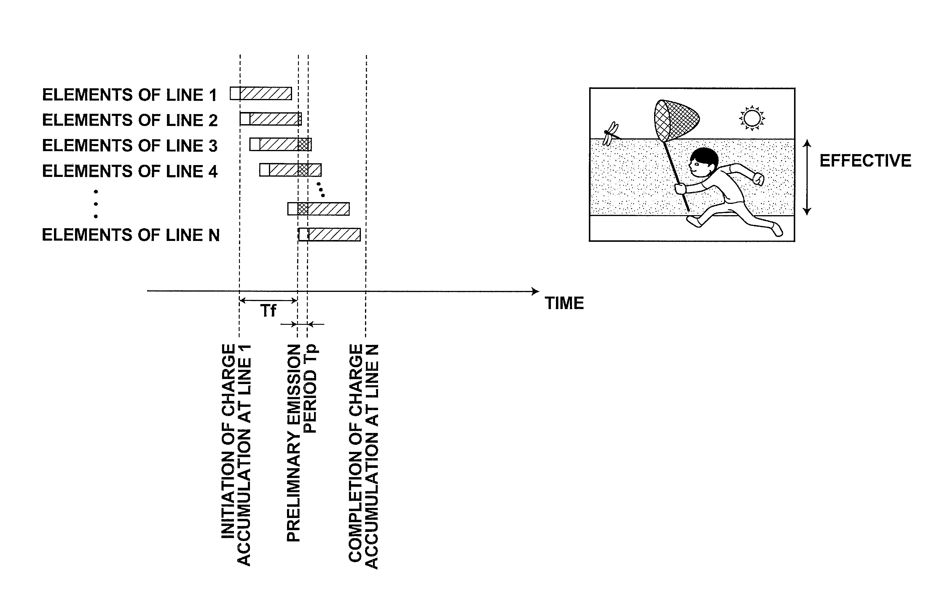
The present invention provides a method for controlling flash emission in an imaging apparatus equipped with a CMOS sensor, even in cases where shutter speed is high. The method involves extracting pixel signals from photoelectric converting elements in which charge accumulation is initiated prior to a preliminary emission period and is ceased after the preliminary emission period. These signals are then used to determine the flash emission amount during the main emission period. The method ensures that the flash emission amount is optimized while complex readout control is avoided. The imaging apparatus includes an image sensor and control means for controlling the charge accumulation timing and the charge accumulation cessation timing of the photoelectric converting elements. The method and apparatus can be used in various applications such as photography, video production, and medical imaging.

Problems solved by technology

On the other hand, CMOS image sensors cannot output signals from all pixels simultaneously due to their structures, unlike CCD image sensors.
This method is effective when the imaging element of the digital camera is a CCD, but not suited for use in the case that the imaging element is a CMOS image sensor, in which the charge accumulation initiation / completion timings are different among pixels.
However, there is a possibility that frequent switching of control methods will lead to problems such as operating errors, which is not preferable.
Therefore, complex processes that accompany frequent switching of control methods is not preferable from the viewpoint of processing time as well.

Method used


Image

  • Imaging apparatus and method for controlling flash emission
  • Imaging apparatus and method for controlling flash emission
  • Imaging apparatus and method for controlling flash emission

Examples


Embodiment Construction

[0030]Hereinafter, an SLR digital camera equipped with a flash photography function and a method for controlling the flash of the digital camera will be described as embodiments of the imaging apparatus and the control method of the present invention.

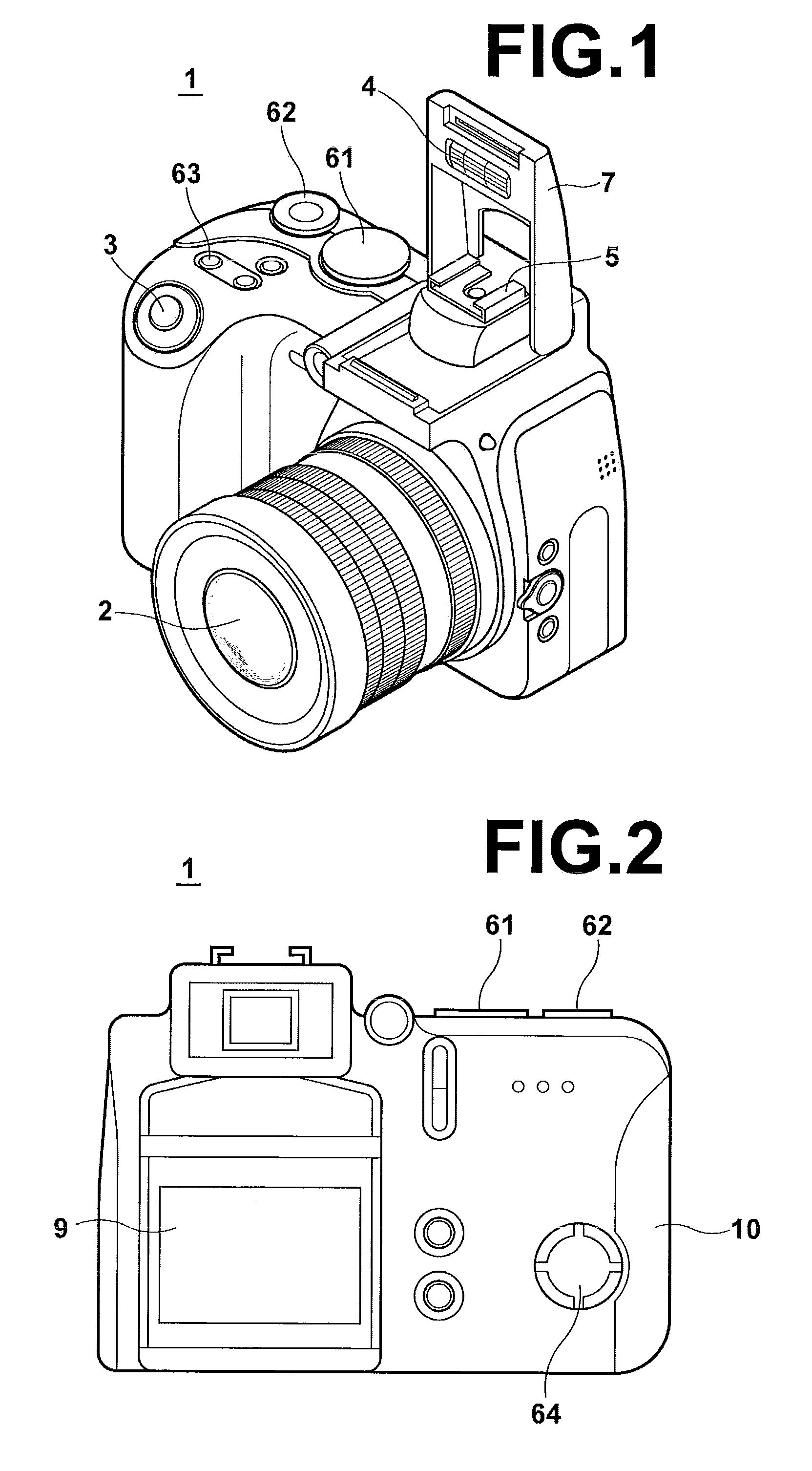
[0031]FIG. 1 is a perspective view that illustrates the outer appearance of a digital camera 1. As illustrated in FIG. 1, an imaging lens 2 is provided on the front surface of the digital camera 1. A shutter release button 3; a flash 4; a hot shoe 5, which is a mounting port for peripheral equipment; and setting / operating buttons 6 that include a mode dial 61 for performing various setting operations; a command dial 62; and a flash button 63 are provided on the upper surface of the digital camera 1.

[0032]The shutter release button 3 is of a structure that can command two types of operations by being depressed in two steps. For example, during a photography operation that utilizes an AE (Automatic Exposure) function and an AF (Automatic ...


PUM


Abstract

An imaging apparatus includes: flash driving means for driving a flash during a set preliminary emission period and a set main emission period; and an image sensor constituted by a plurality of photoelectric converting elements which are arranged in a matrix and capable of being accessed randomly. The charge accumulation initiation timing and the charge accumulation cessation timing of the photoelectric converting elements are controlled line by line or pixel by pixel. The imaging apparatus forms images employing pixel signals output from the photoelectric converting elements, and extracts pixel signals output from photoelectric converting elements in which charge accumulation is initiated prior to the preliminary emission period and ceased after the preliminary emission period. An emission amount to be employed during the main emission period is determined by executing predetermined calculations based on the extracted pixel signals. Main emission of flash is performed with the determined emission amount.

Description

BACKGROUND OF THE INVENTION[0001]1. Field of the Invention[0002]The present invention is related to an imaging apparatus equipped with a flash photography function, and a method for controlling flash. More specifically, the present invention is related to an imaging apparatus that obtains images with an imaging element which is capable of controlling an initiation timing and a cessation timing of charge accumulation in pixel units, and a method, and optimizes flash emission amounts utilizing the images, and a method for optimizing flash emission amounts.[0003]2. Description of the Related Art[0004]Recently, imaging elements which are provided in digital cameras and the like are transitioning form CCD image sensors to CMOS image sensors. CMOS image sensors can be manufactured by a process similar to that for manufacturing CMOS LSI's. Therefore, providing built in circuits other than image sensors into the same chip is facilitated, and CMOS image sensors are suited for use as so calle...

Claims


Application Information

Patent Timeline
Patent Type & Authority Patents(United States)
IPC IPC(8): G03B15/05H04N23/75
CPCG03B15/03
Inventor TAMURA, KAZUNORI
Owner FUJIFILM CORP
Learn More