Semiconductor chip operating with minimal power consumption

a technology of semiconductors and power consumption, applied in the field of semiconductor chips, can solve the problems of wasting power, having difficulty in operating with a minimum necessary power consumption, etc., and achieve the effect of suppressing unnecessary power consumption

Active Publication Date: 2011-10-25
SONY CORP
View PDF10 Cites 3 Cited by
  • Summary
  • Abstract
  • Description
  • Claims
  • Application Information

AI Technical Summary

Benefits of technology

[0019]It is desirable to provide a semiconductor chip that can suppress unnecessary power consumption and operate with a minimum necessary power consumption.
[0030]According to the embodiments of the present invention, it is possible to suppress unnecessary power consumption, and perform operation with a minimum necessary power consumption.

Problems solved by technology

The constitution of FIG. 1 consequently has a disadvantage of having difficulty in operating with a minimum necessary power consumption and wasting power.

Method used


Image

  • Semiconductor chip operating with minimal power consumption
  • Semiconductor chip operating with minimal power consumption
  • Semiconductor chip operating with minimal power consumption

Examples


Embodiment Construction

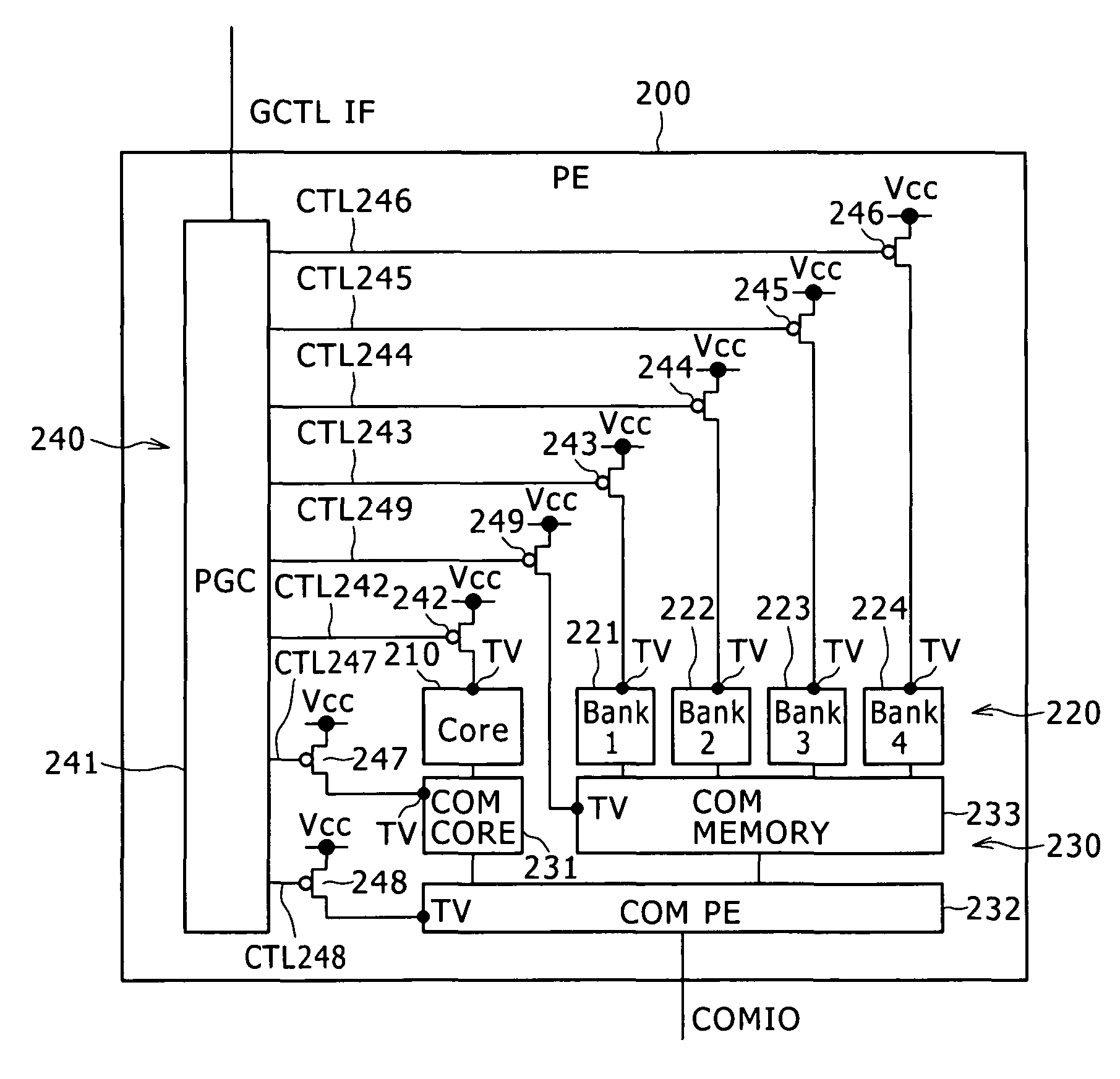
[0037]Preferred embodiments of the present invention will hereinafter be described with reference to the drawings.

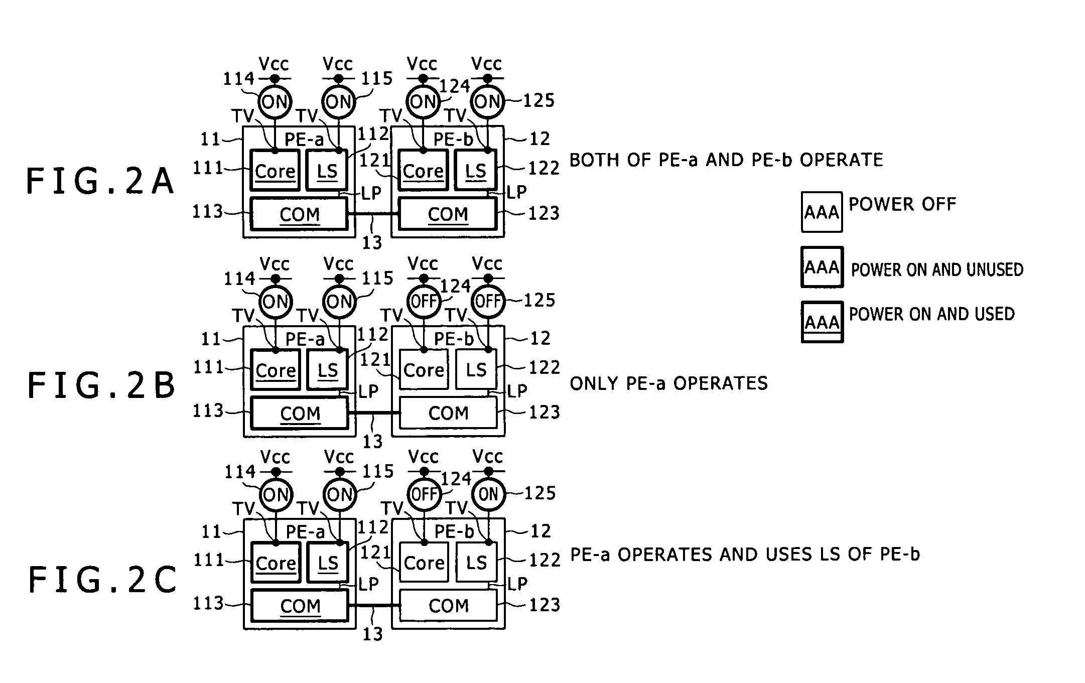
[0038]FIGS. 2A to 2C are diagrams showing an outline of a basic configuration of a semiconductor chip according to an embodiment of the present invention.

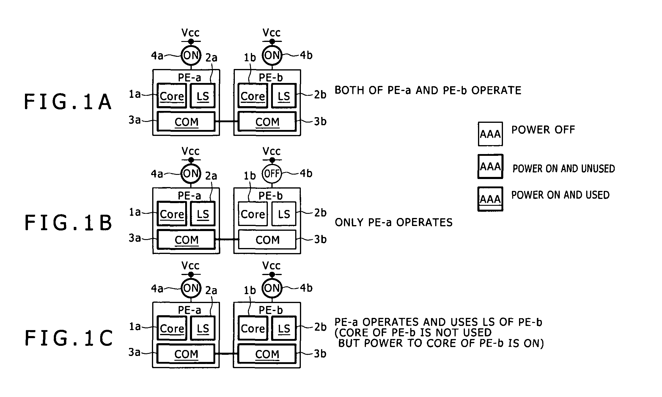
[0039]Description in the following will be made of a case of two PEs. A structure is supposed in which two PEs, that is, PE-a and PE-b are connected to each other by communication units (COM).

[0040]The semiconductor chip 10 in FIGS. 2A to 2C is configured such that two PEs 11 (PE-a) and 12 (PE-b) can lend and borrow an LS (individual memory) to and from each other.

[0041]The PE 11 (PE-a) includes a core 111, an LS 112 of the core 111, and a communication unit (COM) 113. Then, the PE 11 (PE-a) has a power control unit 114 formed by a power gate that is connected between the power supply terminal TV of the core 111 in the PE 11 (PE-a) and a power supply potential Vcc and which can turn on and off the power supply line, and...


PUM


Abstract

Disclosed herein is a semiconductor chip including: a plurality of processing devices that can communicate with each other; wherein each of the processing devices includes an arithmetic unit, an individual memory connected to the arithmetic unit on a one-to-one basis, and a control unit configured to independently control turning on and off of operation of the arithmetic unit and the individual memory.

Description

CROSS REFERENCES TO RELATED APPLICATIONS[0001]The present invention contains subject matter related to Japanese Patent Application JP 2007-316938 filed in the Japan Patent Office on Dec. 7, 2007, the entire contents of which being incorporated herein by reference.BACKGROUND OF THE INVENTION[0002]1. Field of the Invention[0003]The present invention relates to a semiconductor chip including a plurality of processing devices such as processor elements or the like.[0004]2. Description of the Related Art[0005]A semiconductor chip including a plurality of identical processor elements (Processing Elements: PE) is known.[0006]Each PE includes an arithmetic unit (core), an individual memory (LS: Local Storage) connected to the core on a one-to-one basis, and a communication unit (COM) for performing communication with another PE.[0007]Techniques of using the individual memory (LS) of an unused core between PEs, or lending and borrowing the LS of a core between PEs in such a semiconductor sys...

Claims


Application Information

Patent Timeline
Patent Type & Authority Patents(United States)
IPC IPC(8): G06F1/32
CPCG06F1/3203G06F1/3287Y02B60/1278Y02B60/1282Y02D10/00
Inventor OHMORI, MUTSUHIRO
Owner SONY CORP
Why Eureka
Try Eureka