

Through-substrate vias (TSVs) electrically connected to a bond pad design with reduced dishing effect
a technology of through-substrat vias and bond pads, which is applied in the direction of semiconductor devices, semiconductor/solid-state device details, electrical apparatus, etc., can solve the problems of less complex designs, physical limits of the density that can be achieved in two dimensions, and the minimum size needed to make these components, so as to reduce the dishing effect and improve the bonding quality
- Summary
- Abstract
- Description
- Claims
- Application Information
AI Technical Summary
Benefits of technology
Problems solved by technology
Method used
Image

Examples
Embodiment Construction
[0024]The making and using of the presently preferred embodiments are discussed in detail below. It should be appreciated, however, that the present invention provides many applicable inventive concepts that can be embodied in a wide variety of specific contexts. The specific embodiments discussed are merely illustrative of specific ways to make and use the invention, and do not limit the scope of the invention.
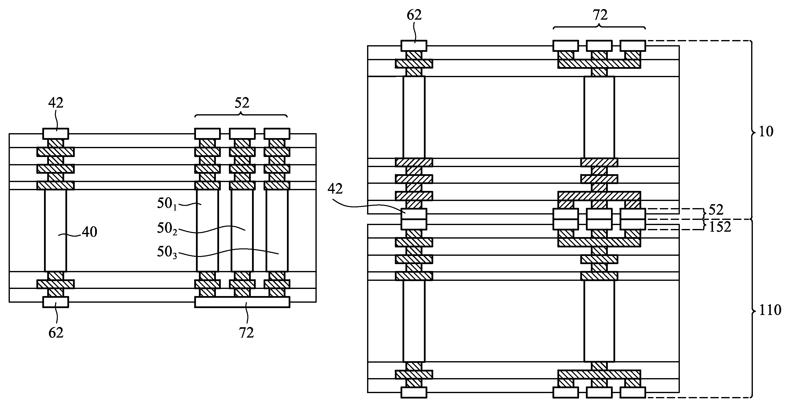
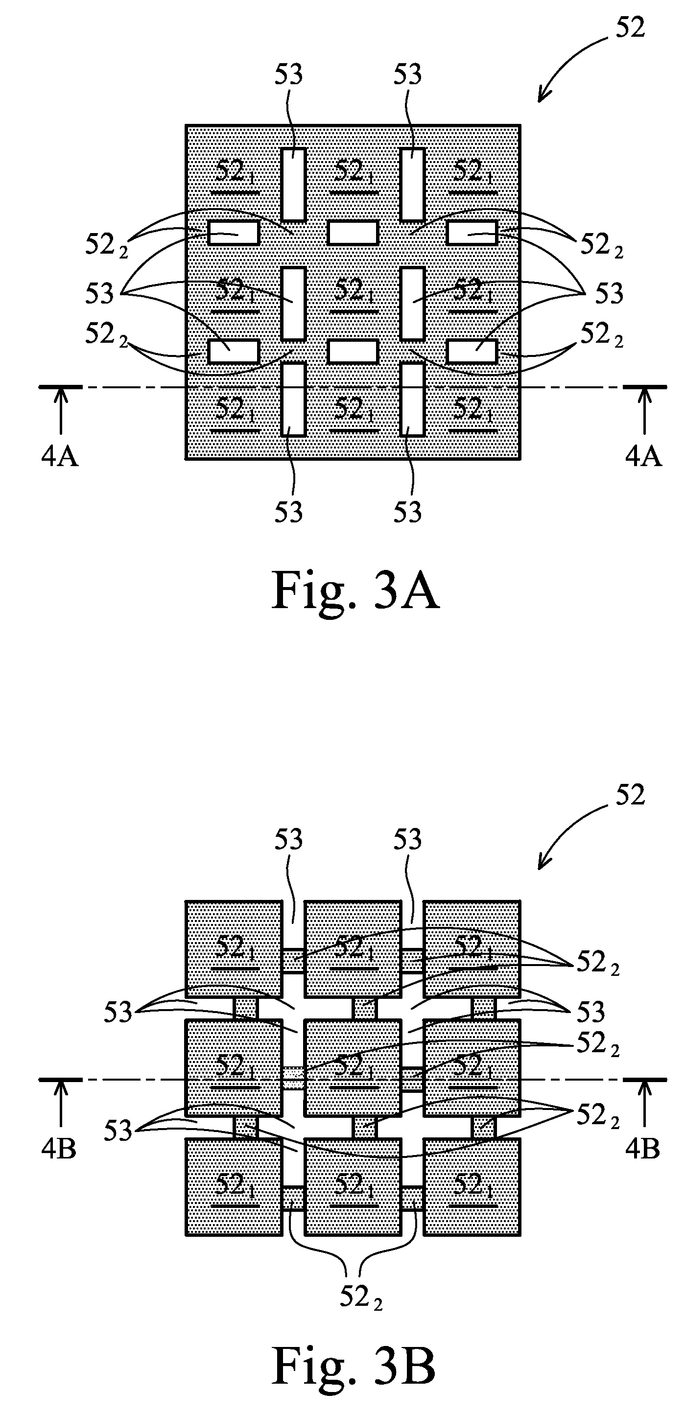
[0025]Generally, an embodiment of the present invention provides an improved bond pad structure for semiconductor chips. An embodiment of the present invention is preferably designed so that the bond pad has slots / openings therein in order to reduce the local pattern density. This is advantageous for minimizing dishing effects. Several embodiments of the present invention will be described herein, which may be used in the context of direct metal-to-metal bonding (often known as direct copper bonding), for example. However, any embodiment of the present invention may also be a...
PUM
 Abstract
Description
Claims
Application Information