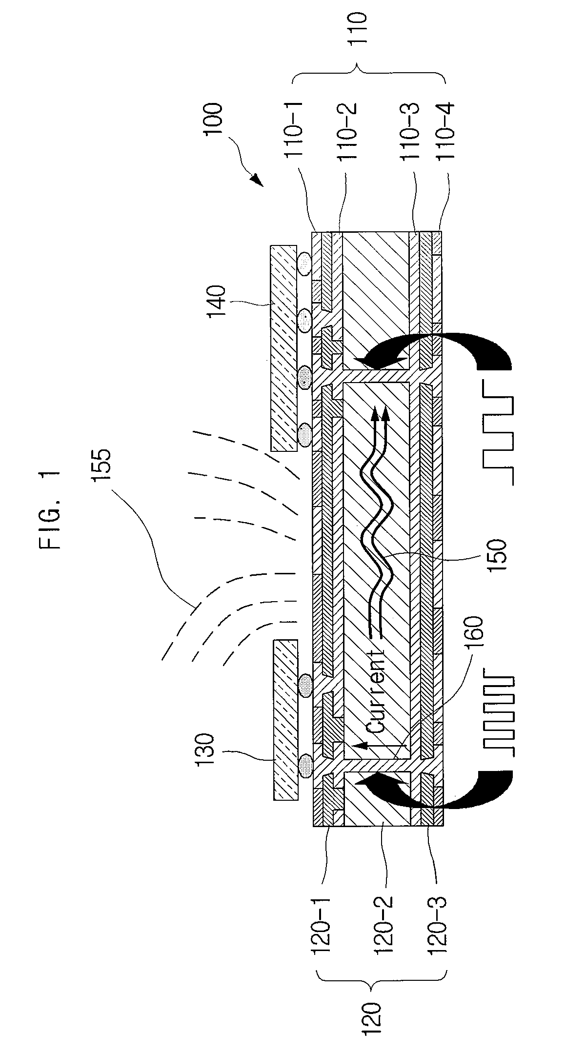
Electromagnetic bandgap structure and printed circuit board
a technology of electromagnetic bandgap and printed circuit board, which is applied in the direction of cross-talk/noise/interference reduction, waveguide type devices, waveguides, etc., can solve the problems of preventing conduction noise, printed circuit board, noise problem, etc., and achieves convenient realization, suitable design flexibility and freedom, and simplified overall process
- Summary
- Abstract
- Description
- Claims
- Application Information
AI Technical Summary
Benefits of technology
Problems solved by technology
Method used
Image

Examples
first embodiment
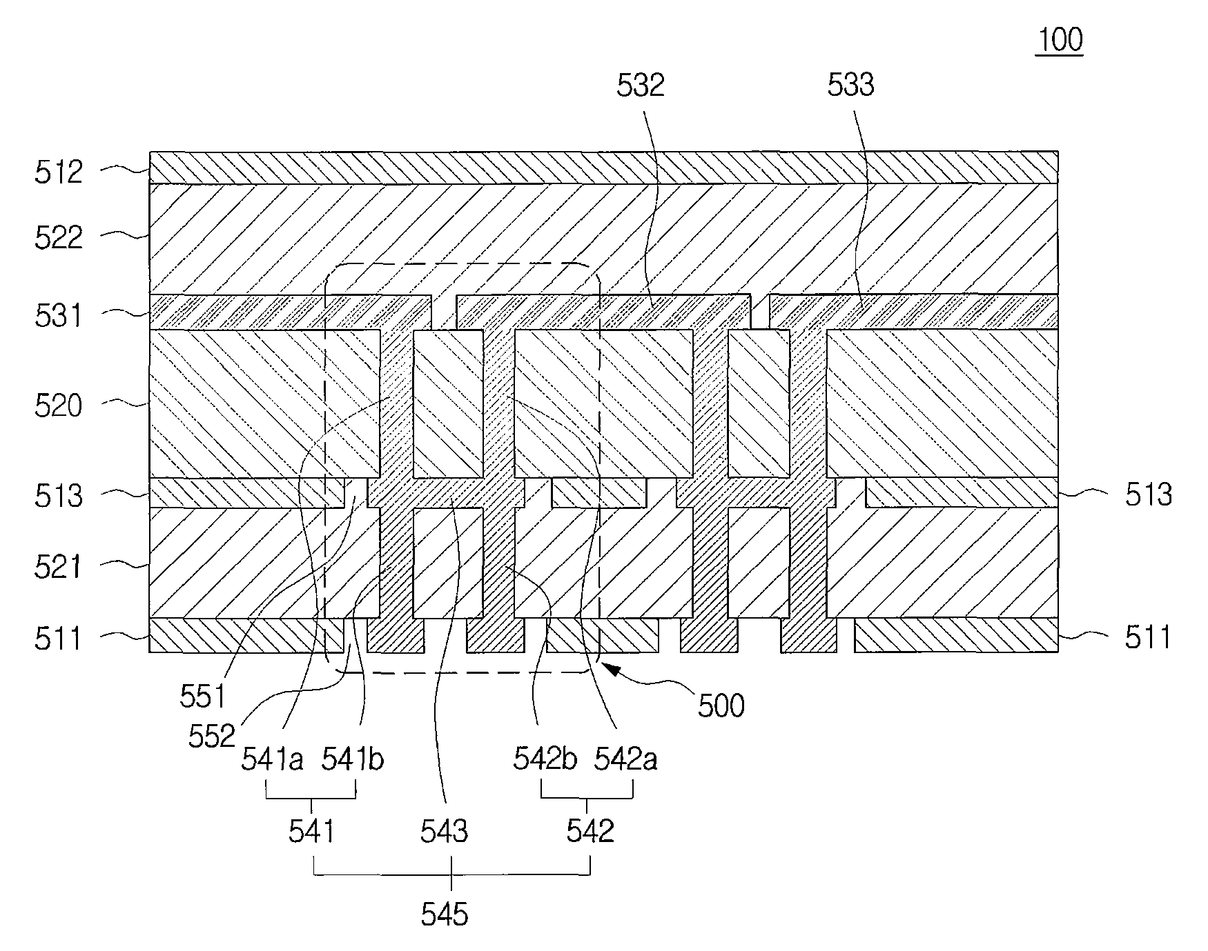
[0137]FIG. 5 is a sectional view showing an electromagnetic bandgap structure including a stitching via and a printed circuit board having the same in accordance with the present invention.
[0138]The electromagnetic bandgap structure in accordance with the first embodiment of the present invention can include a plurality of metal plates placed on a planar surface between two metal layers and stitching vias electrically connecting any two of the metal plates to each other.
[0139]For the convenience of describing the drawings and for an easy comparison with the electromagnetic bandgap structure in FIG. 3A and FIG. 3B, a metal layer represented by reference numeral 511 is dubbed a first metal layer 511. Similarly, metal layers represented by reference numerals 512 and 513, metal plates represented by reference numerals 531, 532 and 533, and dielectric layers represented by reference numerals 520, 521 and 522 are dubbed a second metal layer 512 and a third metal layer 513, a first metal p...
second embodiment
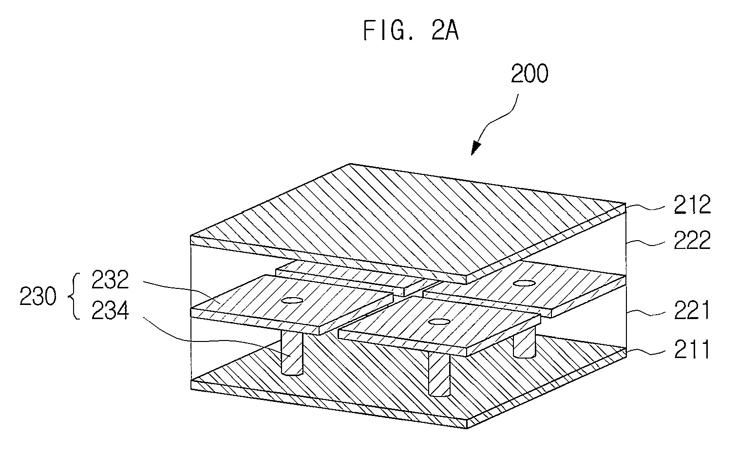
[0155]FIG. 6 is a sectional view showing an electromagnetic bandgap structure including a stitching via and a printed circuit board having the same in accordance with the present invention. FIG. 8A is a 3-D perspective view showing the electromagnetic bandgap structure of FIG. 6.
[0156]The electromagnetic bandgap structure in accordance with the second embodiment of the present invention can include a plurality of metal plates placed on a planar surface between two metal layers and stitching vias electrically connecting any two of the metal plates to each other.
[0157]For the convenience of describing the drawings and for an easy comparison with the electromagnetic bandgap structure in FIG. 3A, FIG. 3B, and FIG. 5, a metal layer represented by reference numeral 611 is dubbed a first metal layer 611. Similarly, metal layers represented by reference numerals 612 and 613, metal plates represented by reference numerals 631, 632 and 633, and dielectric layers represented by reference numer...
third embodiment
[0166]FIG. 7 is a sectional view showing an electromagnetic bandgap structure including a stitching via and a printed circuit board having the same in accordance with the present invention.
[0167]The electromagnetic bandgap structure in accordance with the third embodiment of the present invention can include a plurality of metal plates placed on a planar surface between two metal layers and stitching vias electrically connecting any two of the metal plates to each other.
[0168]For the convenience of describing the drawings and for an easy comparison with the electromagnetic bandgap structure in FIG. 3A, FIG. 3B, FIG. 5, and FIG. 6, a metal layer represented by reference numeral 711 is dubbed a first metal layer 711. Similarly, metal layers represented by reference numerals 712 and 713, metal plates represented by reference numerals 731, 732 and 733, and dielectric layers represented by reference numerals 720, 721 and 722 are dubbed a second metal layer 712 and a third metal layer 713...
PUM
 Abstract
Description
Claims
Application Information