Small outline package in which MOSFET and Schottky diode being co-packaged

a diode and small outline technology, applied in the direction of semiconductor devices, semiconductor/solid-state device details, electrical apparatus, etc., can solve the problems of limiting the voltage conversion efficiency, affecting the efficiency of the voltage converter, and the packaging configuration encounters several technical difficulties, so as to improve the dc-dc conversion efficiency, simplify the external connection, and shorten the current path

Active Publication Date: 2012-01-03
ALPHA & OMEGA SEMICON LTD
View PDF9 Cites 14 Cited by
  • Summary
  • Abstract
  • Description
  • Claims
  • Application Information

AI Technical Summary

Benefits of technology

[0009]Specifically, it is an aspect of the present invention to provide an improved TSOP package configuration to contain a MOSFET device with a Schottky diode by arranging the D terminal on the same side as the K-terminal of the Schottky diode to simplify the external connection such that the current path may be shortened. Improvement of DC-DC conversion efficiency is achieved with shortened current path. The circuit designs are simplified and the battery life is extended with improved conversion efficiency and shorter current path.
[0010]In order to achieve these purposes, a new and improved TSOP package is disclosed. The package includes a leadframe with a second lead for an S-terminal of a MOSFET device contained therein. A third lead of the leadframe is for the G-terminal of the MOSFET and the fourth lead is for the D1 terminal of the MOSFET, and the fifth lead for the D2 terminal of the MOSFET wherein the D2 terminal may be a backup terminal for the D1 terminal of the MOSFET device. The fourth lead of D1 terminal is connected to the first carrier plate of the MOSFET such that the D terminal of the MOSFET is on the same side with the K-terminal of the Schottky diode. Specifically, the first lead of the leadframe is for the K terminal of the Schottky diode and is connected to the second carrier plate for supporting the Schottky diode and the sixth lead is for the A terminal of the Schottky diode. With such layout configuration, the current path is significantly shortened. The voltage conversion efficiency is improved. The complexity of the lead arrangements in a printed circuit board (PCB) is also simplified. The sixth lead for the A-terminal has a T-shape structure. The second lead for wire bonding has a L-shape structure thus enhancing the security of wire attachment with increased wire bonding areas. The fifth lead is connected to the carrier plate for the MOSFET thus improves the heat dissipation and further improves the structural integrity. The length for wire bonding of the sixth lead may be extended for increasing the numbers of wires bonded to the area.

Problems solved by technology

However, such packaging configuration encounters several technical difficulties when implemented in a DC-DC converter with the circuit diagram shown in FIG. 1.
Since a longer current path would adversely affect efficiency of the voltage converter, the conventional packaging configuration as shown limits the voltage conversion efficiency.
Additionally, a current path further complicates the circuit design thus adversely affects the design processes and also the production cost of the DC-DC converter.

Method used


Image

  • Small outline package in which MOSFET and Schottky diode being co-packaged
  • Small outline package in which MOSFET and Schottky diode being co-packaged
  • Small outline package in which MOSFET and Schottky diode being co-packaged

Examples


Embodiment Construction

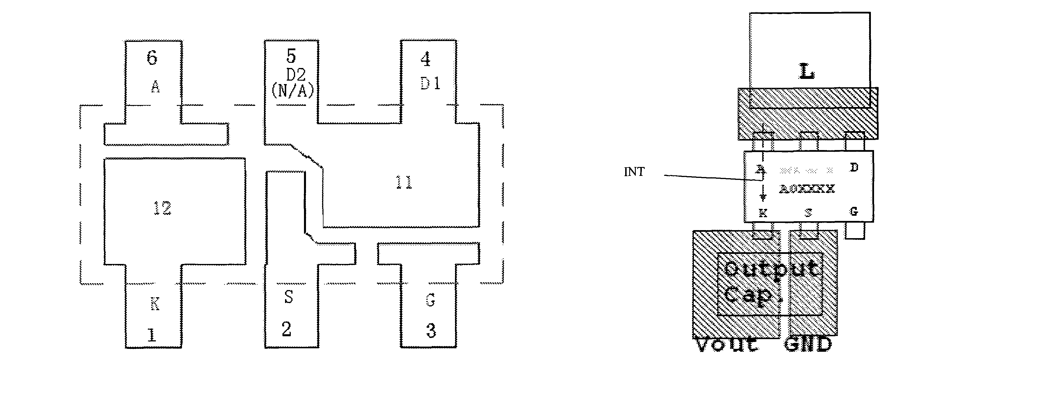
[0018]Referring to FIGS. 4 to 5 for a six-lead TSOP package containing a MOSFET device and Schottky diode as a preferred embodiment of this invention.

[0019]Referring to FIG. 4 for the six-lead TSOP package containing a MOSFET device and Schottky diode that includes a leadframe 10 having six leads. The second lead 2 of the lead frame is for the S terminal of the MOSFET device, the third lead 3 of the lead frame is for the G-terminal of the MOSFET, the fourth lead 4 of the lead frame is for the D1 terminal of the MOSFET, the fifth lead 5 of the leadframe is either an open ended lead or may be a backup connection to D2 terminal of the MOSFET that may not be necessary depending the applications in different portable electronic devices. The fourth lead 4 of the lead frame for the D1 terminal of the MOSFET is also connected to the carrier plate 11 of the MOSFET 20 as shown in FIG. 6. Furthermore, the fourth lead 4 of the leadframe and the sixth lead 6 of the leadframe for the A terminal o...


PUM


Abstract

A TSOP (Thin Small Outline Package) contains a MOSFET and a Schottky diode. The MOSFET has a source terminal a gate terminal and a drain terminal. The Schottky diode has a cathode terminal, a anode terminal. The TSOP contains the MOSFET and the Schottky diode with a special configuration by placing the drain terminal of the MOSFET and the anode terminal of the Schottky diode on a same side. Specifically, the TSOP implements a leadframe that comprises a plurality of leads. The drain terminal of the MOSFET and the anode terminal extends outside of the TSOP separate on the same side of the package.

Description

[0001]This application claims priority to pending PCT Application PCT / CN2005 / 001658 filed on Oct. 9, 2005 claiming a Priority date of Oct. 30, 2004 filed by the Applicants of this Patent Application.BACKGROUND OF THE INVENTION[0002]1. Field of the Invention[0003]The invention disclosed herein relates generally to a compact packaging configuration with narrow package width. More particularly, this invention relates to a novel and improved device layout and packaging configuration for combining a metal oxide semiconductor field effect transistor (MOSFET) and a Schottky diode into a narrow and compact TSOP (thin small outline package).[0004]2. Description of the Prior Art[0005]Referring to FIG. 1 for a DC-to-DC power converter that is becoming increasingly more important because such devices are now being implemented in more and more portable power electronic devices. Conventional packages combine a narrow MOSFET device 20′ with a Schottky diode 30′ into a dual-chip leadframe package a...

Claims


Application Information

Patent Timeline
Patent Type & Authority Patents(United States)
IPC IPC(8): H01L23/495
CPCH01L23/49562H01L23/49575H01L25/165H01L2924/13091H01L2924/0002H01L2924/00
Inventor SHI, ZHENGYUWANG, LIMINSHI, LEI
Owner ALPHA & OMEGA SEMICON LTD
Why Eureka
Try Eureka