Inertial sensor

a sensor and inertial sensor technology, applied in the field ofinertial sensors, to achieve the effect of suppressing fixation, suppressing the s/n ratio reduction of the sensor output and offset occurren

Active Publication Date: 2012-01-17
HITACHI LTD
View PDF10 Cites 7 Cited by
  • Summary
  • Abstract
  • Description
  • Claims
  • Application Information

AI Technical Summary

Benefits of technology

[0013]As described in the Patent Document 1 above, a stopper has been conventionally provided in order to prevent the fixation between the movable electrode and the fixed electrode. When the effective area by which the movable electrode surface and the fixed electrode surface contact with each other is reduced by providing the stopper, the possibility of generation of the induced charge or induced polarization on the electrode surfaces upon occurrence of the fixation can be reduced and the electrostatic force between the movable electrode and the fixed electrode via the electrically insulating films can be suppressed.
[0016]Therefore, an object of the present invention is to provide techniques capable of suppressing fixation between a movable electrode and a fixed electrode in an inertial sensor and preventing the inertial sensor from malfunctioning.
[0017]Also, another object of the present invention is to provide techniques capable of suppressing S / N ratio reduction of the sensor output and offset occurrence caused by the parasitic capacitance between a fixed electrode and a peripheral conductor in an inertial sensor.
[0024](1) The fixation between the movable electrode and the fixed electrode can be suppressed, and the inertial sensor can be prevented from malfunctioning without increasing the number of fabrication processes of the inertial sensor.
[0025](2) The S / N ratio reduction of the sensor output and offset occurrence caused by the parasitic capacitance between the fixed electrode and the peripheral conductor can be suppressed.
[0026](3) The S / N ratio reduction of the sensor output and the offset occurrence can be suppressed by suppressing leakage of a drive signal to a detection signal caused by capacitive coupling of the drive electrode and the detection electrode.

Problems solved by technology

For example, during a fabrication process or when a sensor chip is to be mounted on a package, if a high voltage is applied to the sensor chip for some reason and static electricity is stored in the inertial body or if a charged external object and the sensor chip contact each other and static electricity is stored in the inertial body, static electricity force is generated between the movable electrodes and the fixed electrodes, the movable electrodes are attracted to the fixed electrodes, and the both electrodes are fixed to each other, thereby causing malfunction.
Even after the voltage from outside is removed, the electric charge distribution sometimes remains on the insulating surfaces, and the electrostatic force between the movable electrodes and the fixed electrodes via the electrically insulating films remains, thereby causing malfunction.

Method used


Image

  • Inertial sensor
  • Inertial sensor
  • Inertial sensor

Examples


first embodiment

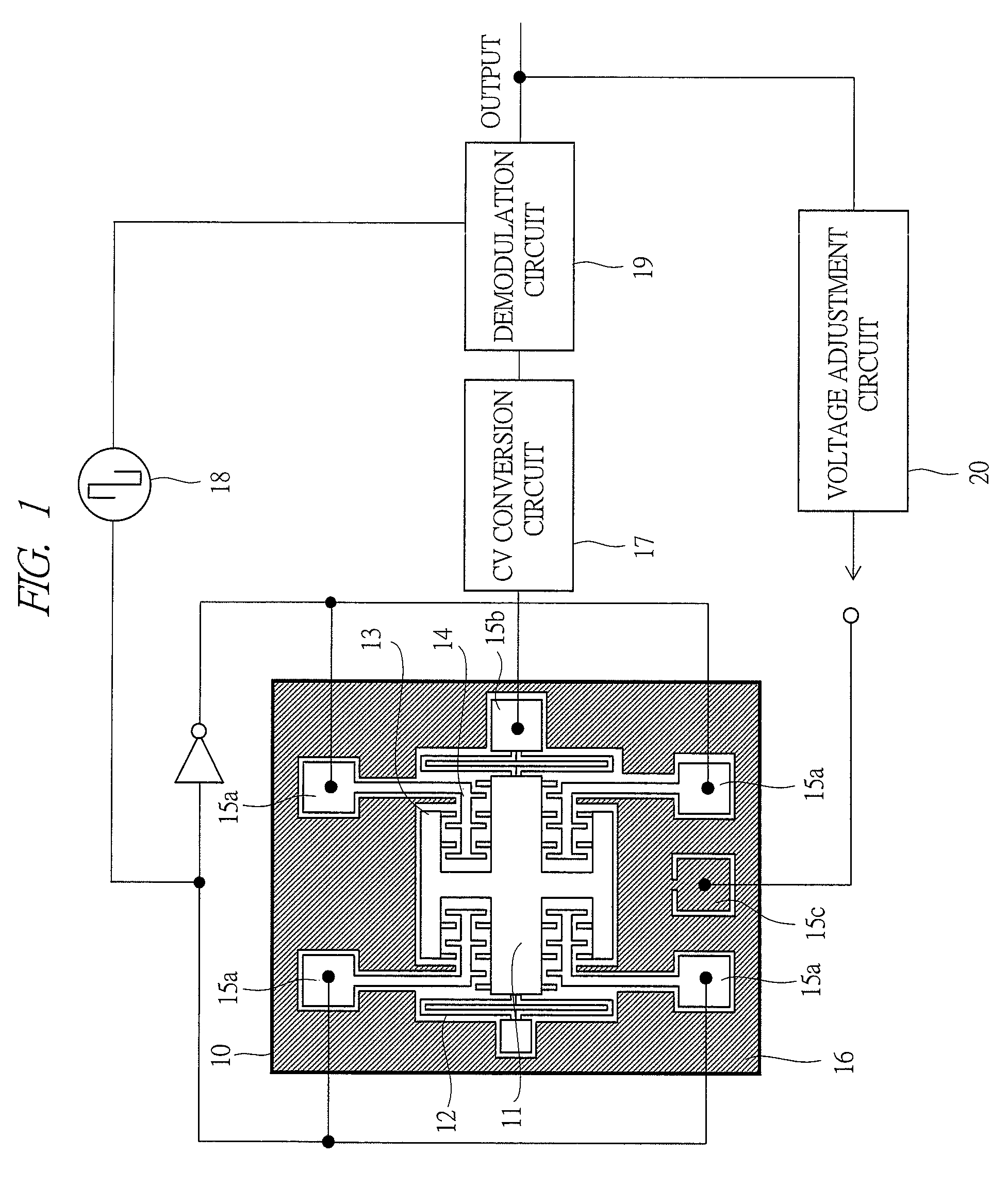
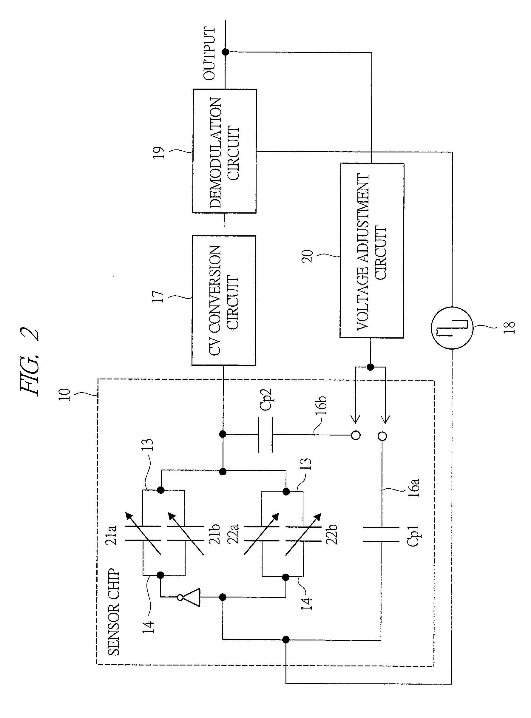
[0046]FIG. 1 shows a schematic diagram of a chip overview and wiring of an acceleration sensor according to a first embodiment of the present invention.

[0047]The acceleration sensor serving as an inertial sensor according to the first embodiment comprises: a sensor chip 10; a capacitance / voltage (CV) conversion circuit 17 serving as a detection circuit; a carrier-wave application circuit 18; a demodulation circuit 19; a voltage adjustment circuit 20 serving as a control circuit; and others. An inertial mass 11, supporting beam structures 12 of the inertial body, movable electrodes 13 and fixed electrodes 14 for detecting the travel distance of the inertial body, and pad patterns 15a to 15c for connecting the sensor chip 10 with detection circuit elements are formed on the sensor chip 10. In addition, a peripheral conductor 16 is provided so as to surround the peripheries of these sensor constituent elements. Further, the fixed electrodes 14 are provided to face the movable electrode...

second embodiment

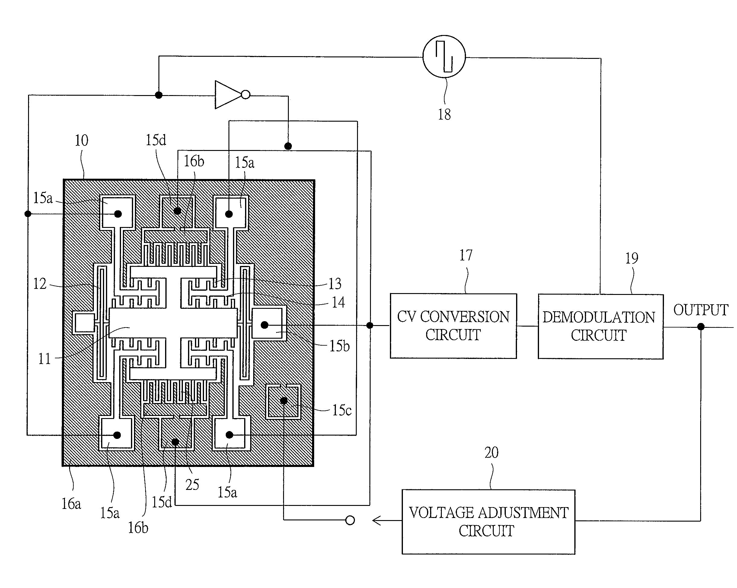
[0057]FIG. 4 shows a schematic diagram of a chip overview and wiring of an acceleration sensor according to a second embodiment of the present invention.

[0058]The acceleration sensor serving as an inertial sensor according to the second embodiment comprises: the sensor chip 10; the capacitance / voltage (CV) conversion circuit 17 serving as a detection circuit; the carrier-wave application circuit 18; the demodulation circuit 19; the voltage adjustment circuit 20 serving as a control circuit; and others. The inertial mass 11, the supporting beam structures 12 of the inertial body, the movable electrodes 13 and the fixed electrodes 14 for detecting the travel distance of the inertial body, restriction means 25 which restricts the operation of the acceleration sensor, and pad patterns 15a to 15d for connecting the sensor chip 10 with detection circuit elements are formed on the sensor chip 10. In addition, the peripheral conductors 16a and 16b are provided so as to surround the peripher...

third embodiment

[0068]FIG. 7 shows a chip overview and wiring of an acceleration sensor according to a third embodiment of the present invention.

[0069]The acceleration sensor serving as an inertial sensor according to the third embodiment comprises: the sensor chip 10; the capacitance / voltage (CV) conversion circuit 17 serving as a detection circuit; the carrier-wave application circuit 18; the demodulation circuit 19; the voltage adjustment circuit 20 serving as a control circuit; and others. The inertial mass 11, the supporting beam structures 12 of the inertial body, the movable electrodes 13 and the fixed electrodes 14 for detecting the travel distance of the inertial body, and pad patterns 15a to 15c and 15e for connecting the sensor chip 10 with detection circuit elements are formed on the sensor chip 10. Also, the conductor 16 is provided so as to surround the peripheries of these sensor constituent elements. When acceleration is applied to the sensor, the inertial mass 11 is displaced in th...


PUM


Abstract

Techniques capable of suppressing fixation between a movable electrode and a fixed electrode in an inertial sensor and preventing the inertial sensor from malfunctioning are provided. The movable electrode, the fixed electrode provided so as to face the movable electrode, a peripheral conductor facing both the movable electrode and the fixed electrode, and a demodulation circuit and a voltage adjustment circuit which adjust the electric potential of the peripheral conductor so that the electric potential of the peripheral conductor becomes the same as the electric potential of the movable electrode are provided, and a change in the capacitance between the movable electrode and the fixed electrode is detected.

Description

CROSS-REFERENCE TO RELATED APPLICATION[0001]The present application claims priority from Japanese Patent Application No. JP 2007-299210 filed on Nov. 19, 2007 and Japanese Patent Application No. JP 2008-223182 filed on Sep. 1, 2008, the contents of which are hereby incorporated by reference into this application.TECHNICAL FIELD OF THE INVENTION[0002]The present invention relates to a semiconductor physical quantity sensor, and in particular to an inertial sensor fabricated by using Micro-Electro-Mechanical Systems (MEMS) techniques and used in detection of a change of electrostatic capacitance.BACKGROUND OF THE INVENTION[0003]As the techniques studied by the inventors of the present invention, for example, following techniques are conceivable in an inertial sensor.[0004]By virtue of progresses in semiconductor processing techniques and micro machining techniques (so-called MEMS techniques), a MEMS inertial sensor element which has a detection circuit and detects physical quantities ...

Claims


Application Information

Patent Timeline
Patent Type & Authority Patents(United States)
IPC IPC(8): G01C19/56
CPCG01C19/5726G01P15/125G01C19/5755G01P2015/0814
Inventor YAMANAKA, KIYOKOJEONG, HEEWON
Owner HITACHI LTD
Why Eureka
Try Eureka