Eureka AIR delivers breakthrough ideas for toughest innovation challenges, trusted by R&D personnel around the world.

Semiconductor chip fabrication method

a technology of semiconductor chips and fabrication methods, applied in semiconductor/solid-state device manufacturing, basic electric elements, electric apparatus, etc., can solve the problems of short cutting blade life, inconvenient fabrication of semiconductor chips, and inability to form modified layers inside metal films

Active Publication Date: 2012-01-24
DISCO CORP
View PDF6 Cites 1 Cited by
  • Summary
  • Abstract
  • Description
  • Claims
  • Application Information

AI Technical Summary

Benefits of technology

[0008]It is therefore an object of the present invention to provide a semiconductor chip fabrication method which can divide a semiconductor wafer having a metal film on the back side into the individual semiconductor chips efficiently without the generation of processing dust or contamination.
[0011]According to the present invention, the modified layer is formed inside the semiconductor wafer along each street by applying the laser beam. Thereafter, the metal film as a ground is formed on the back side of the semiconductor wafer. Thereafter, the semiconductor wafer with the metal film is divided into the individual semiconductor chips along the modified layer formed along each street. Accordingly, although the metal film as a ground is formed on the back side of the semiconductor wafer, the semiconductor wafer can be divided into the individual semiconductor chips efficiently without the generation of processing dust or contamination. Further, as compared with a method of cutting a semiconductor wafer along each street as by dicing using a cutting blade, the ratio in area of all the streets to the device area can be reduced to thereby improve the production efficiency.

Problems solved by technology

Furthermore, there is another problem that metal dust or contamination may adhere to the cutting blade to cause clogging of the cutting blade, resulting in a short life of the cutting blade.
On the other hand, in the laser processing method using a pulsed laser beam having a transmission wavelength to the semiconductor wafer, a modified layer cannot be formed inside the metal film because the laser beam is not transmitted through the metal film.
However, in both methods, processing dust or contamination called melt residues or debris is generated, so that these methods are not suitable for the fabrication of semiconductor chips required to avoid such processing dust or contamination.

Method used


Image

  • Semiconductor chip fabrication method
  • Semiconductor chip fabrication method
  • Semiconductor chip fabrication method

Examples


Embodiment Construction

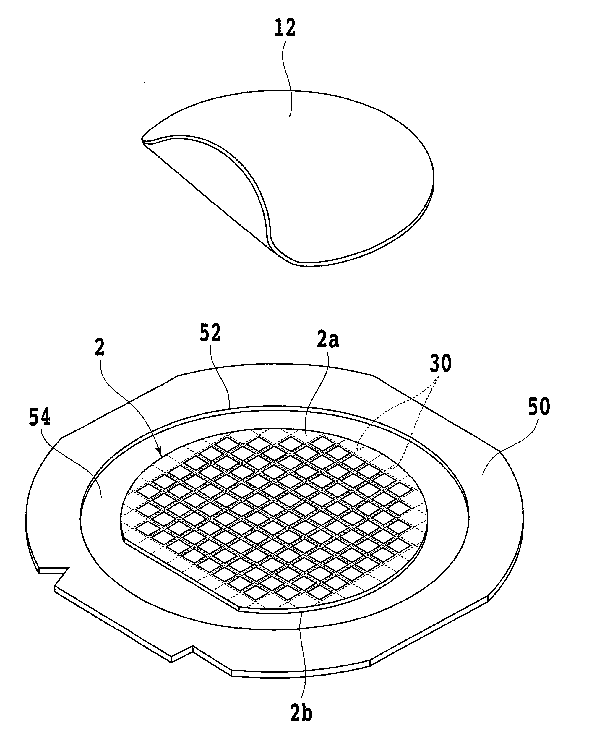
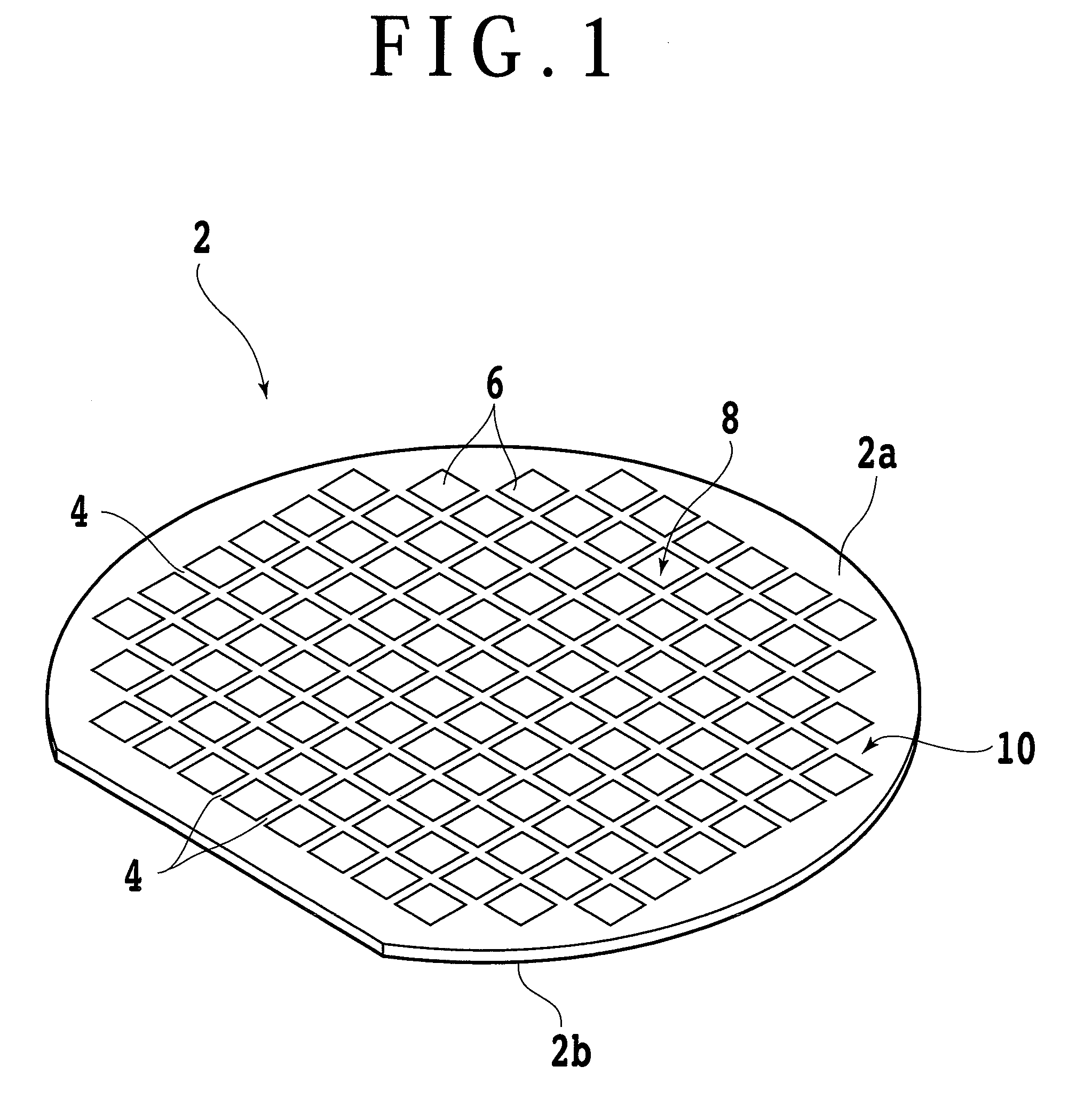
[0024]A preferred embodiment of the semiconductor chip fabrication method according to the present invention will now be described in detail with reference to the attached drawings. FIG. 1 is a perspective view of a semiconductor wafer 2 as viewed from the front side 2a thereof. For example, the semiconductor wafer 2 is a silicon wafer having a thickness of 300 μm. The front side 2a of the semiconductor wafer 2 is formed with a plurality of crossing streets (division lines) 4 to thereby define a plurality of partitioned regions arranged like a matrix, and a plurality of devices 6 such as ICs and LSIs are formed in these partitioned regions.

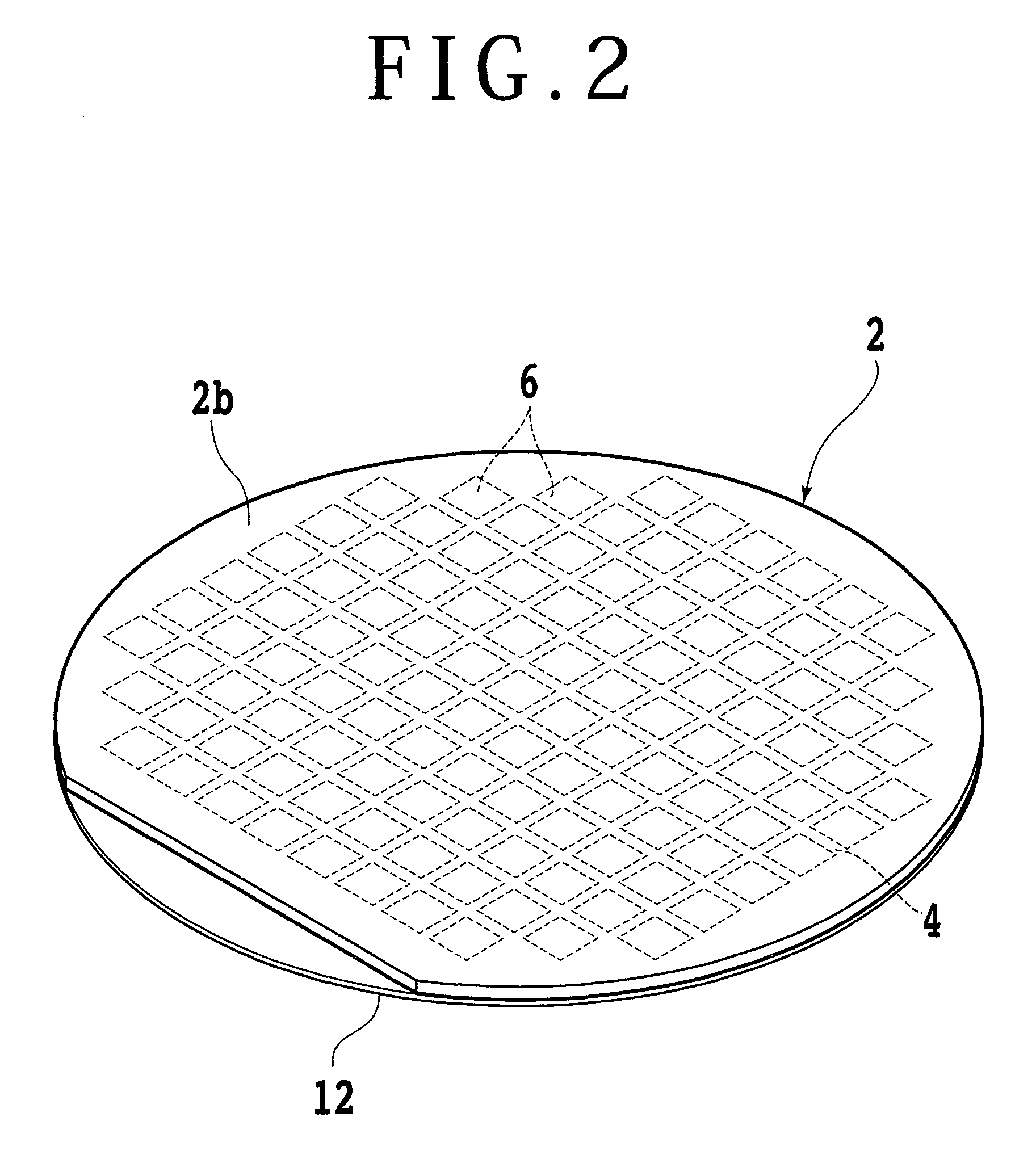
[0025]The semiconductor wafer 2 includes a device area 8 where the devices 6 are formed and a marginal area 10 surrounding the device area 8. As shown in FIG. 2, a protective tape 12 is attached to the front side 2a of the semiconductor wafer 2 in a protective tape attaching step. Accordingly, the front side 2a of the semiconductor wafer 2 is prot...


PUM

PropertyMeasurementUnit
thicknessaaaaaaaaaa
thicknessaaaaaaaaaa
sizeaaaaaaaaaa

Abstract

A semiconductor chip fabrication method including a modified layer forming step of applying a laser beam having a transmission wavelength to the semiconductor wafer from the back side of the semiconductor wafer along the streets formed on the front side of the semiconductor wafer so that a focal point of the laser beam is set inside the semiconductor wafer, thereby forming a modified layer in the semiconductor wafer along each street, a metal film deposition step of depositing a metal film on the back side of the semiconductor wafer after the modified layer forming step, a semiconductor wafer attaching step of attaching the semiconductor wafer to an adhesive tape supported to an annular frame, and a semiconductor wafer dividing step of applying an external force to the semiconductor wafer in the condition where the semiconductor wafer is attached to the adhesive tape to thereby divide the semiconductor wafer with the metal film into the individual semiconductor chips along the modified layer formed along each street.

Description

BACKGROUND OF THE INVENTION[0001]1. Field of the Invention[0002]The present invention relates to a semiconductor chip fabrication method for dividing a semiconductor wafer into individual semiconductor chips (devices) along a plurality of crossing streets formed on the front side of the semiconductor wafer, wherein the devices are respectively formed in a plurality of regions partitioned by the streets and the back side of the semiconductor wafer is coated with a metal film.[0003]2. Description of the Related Art[0004]A plurality of devices such as ICs and LSIs are formed on the front side of a semiconductor wafer. The back side of the semiconductor wafer is ground to obtain a desired thickness of the semiconductor wafer. Thereafter, the semiconductor wafer is divided along a plurality of crossing streets (division lines) to obtain the individual semiconductor chips, which are used in various electronic equipment. In general, the semiconductor wafer is divided into the individual se...

Claims


Application Information

Patent Timeline
Patent Type & Authority Patents(United States)
IPC IPC(8): H01L21/78
CPCH01L21/78H01L21/30
Inventor NAGASAWA, TADATO
Owner DISCO CORP
Why Eureka
Eureka Blog
Learn More