

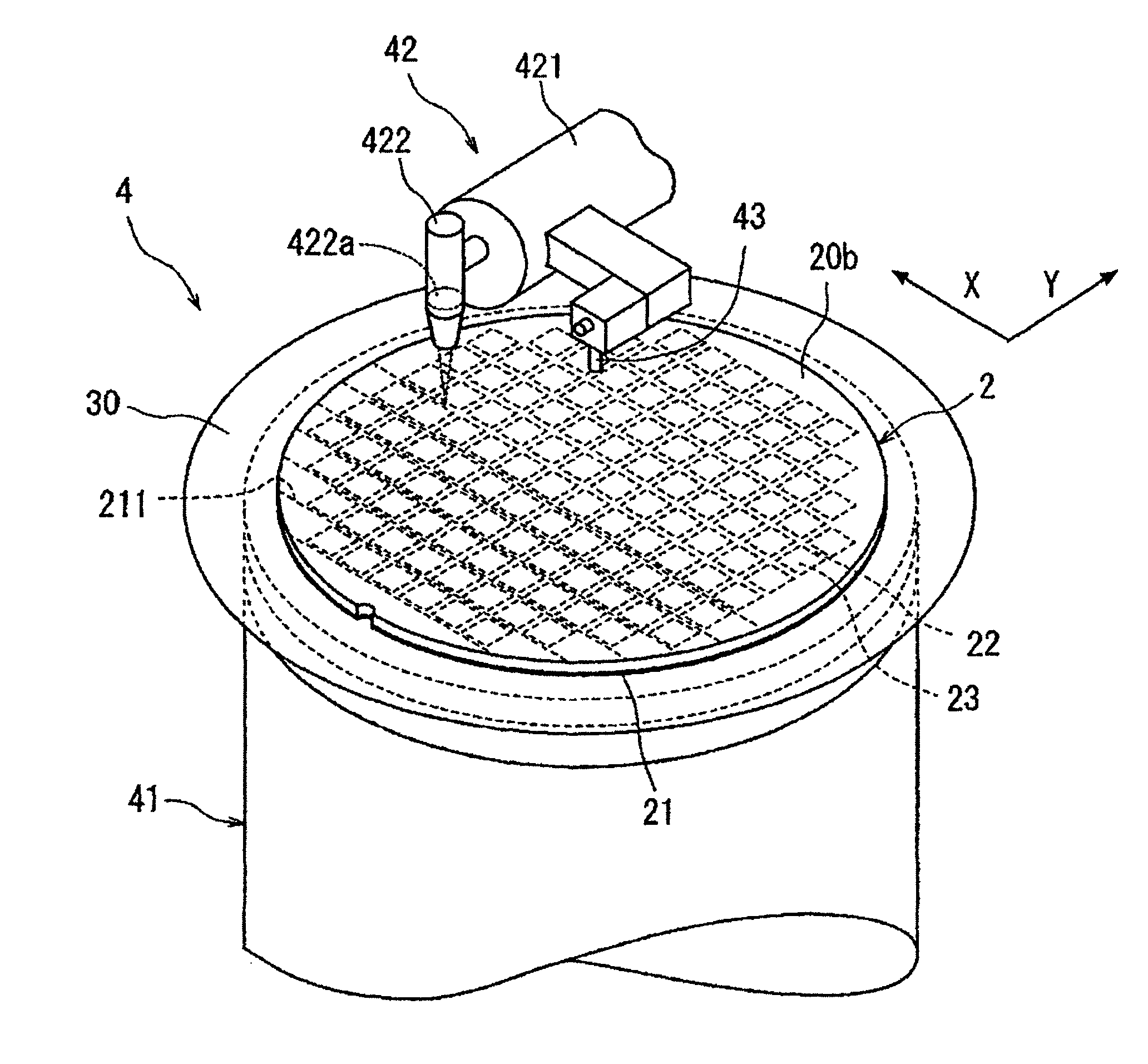
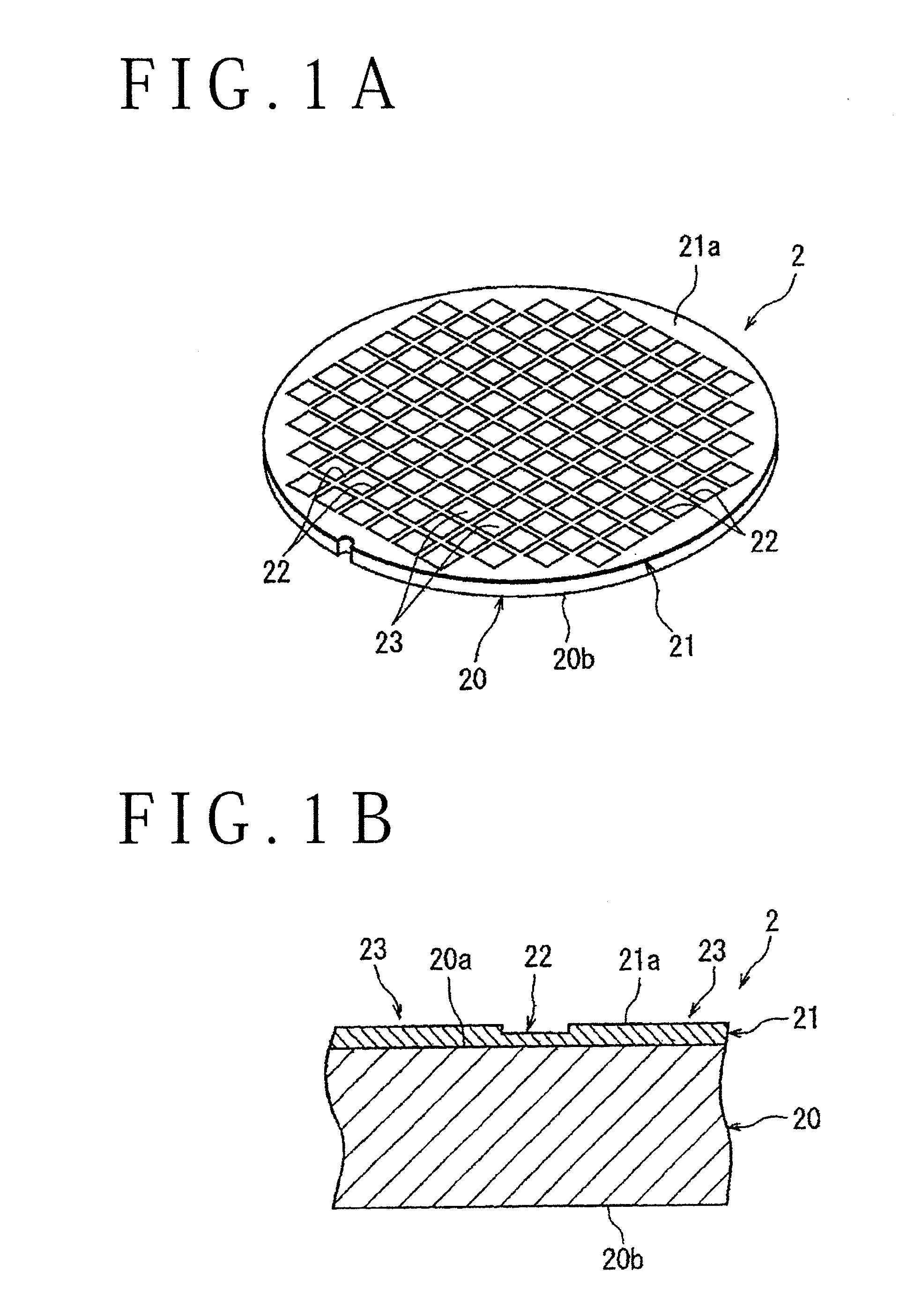
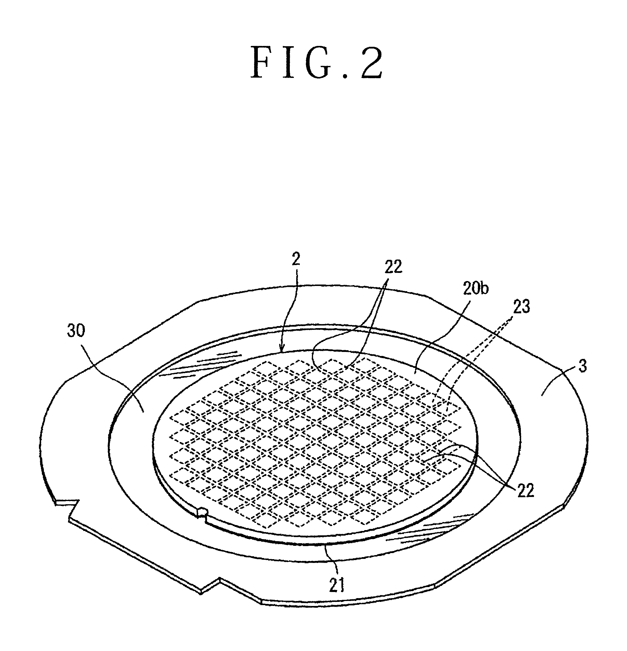
Optical device wafer processing method
a technology of optical devices and processing methods, applied in the direction of semiconductor/solid-state device manufacturing, semiconductor devices, electrical apparatus, etc., can solve the problems of productivity reduction, quality degradation, and productivity reduction of optical devices, and achieve the effect of greatly improving productivity
- Summary
- Abstract
- Description
- Claims
- Application Information
AI Technical Summary
Benefits of technology
Problems solved by technology
Method used
Image

Examples
example 1-1
[0058]By using a sapphire (Al2O3) substrate (refractive index: 1.7) having a thickness of 1000 μm, the shield tunnel forming step was performed under the following processing conditions to form a shield tunnel, and it was determined whether or not the shield tunnel is good.
Processing Conditions
[0059]Wavelength: 1030 nm
[0060]Repetition frequency: 50 kHz
[0061]Pulse width: 10 ps
[0062]Average power: 3 W
[0063]Focused spot diameter: 10 μm
[0064]Work feed speed: 500 mm / s
Numerical aperture(NA) of theGood / poor condition offocusing lensthe shield tunnelS = NA / N0.05Not formed0.1Slightly good0.0580.15Good0.0880.2Good0.1170.25Good0.1470.3Good0.1760.35Slightly good0.2050.4Poor0.45Poor: voids generated0.5Poor: voids generated0.55Poor: voids generated0.6Poor: voids generated
[0065]It is apparent from the above results that in the case of using a sapphire (Al2O3) substrate (refractive index: 1.7) as the single crystal substrate a substantially good shield tunnel can be formed by setting the numerical ...
example 1-2
[0066]By using a silicon carbide (SiC) substrate (refractive index: 2.63) having a thickness of 1000 μm, the shield tunnel forming step was performed under the following processing conditions to form a shield tunnel, and it was determined whether or not the shield tunnel is good.
Processing Conditions
[0067]Wavelength: 1030 nm
[0068]Repetition frequency: 50 kHz
[0069]Pulse width: 10 ps
[0070]Average power: 3 W
[0071]Focused spot diameter: 10 μm
[0072]Work feed speed: 500 mm / s
Numerical aperture(NA) of theGood / poor condition offocusing lensthe shield tunnelS = NA / N0.05Not formed0.1Not formed0.15Slightly good0.0570.2Good0.0760.25Good0.0950.3Good0.1140.35Good0.1330.4Good0.1530.45Good0.1710.5Good0.190.55Slightly good0.2090.6Poor: voids generated
[0073]It is apparent from the above results that in the case of using a silicon carbide (SiC) substrate (refractive index: 2.63) as the single crystal substrate a substantially good shield tunnel can be formed by setting the numerical aperture (NA) of th...
example 2
[0077]The pulsed laser beam was applied to a sapphire (Al2O3) substrate and silicon carbide (SiC) substrate each having a thickness of 1000 μm under the following processing conditions to determine the relation between the energy (μJ / pulse) of the pulsed laser beam and the length (μm) of the shield tunnel.
Processing Conditions
[0078]Wavelength: 1030 nm
[0079]Repetition frequency: 50 kHz
[0080]Pulse width: 10 ps
[0081]Focused spot diameter: 10 μm
[0082]Work feed speed: 500 mm / s
[0083]The average power of the pulsed laser beam was increased from 0.05 W (1 μJ / pulse) at intervals of 0.05 W (1 μJ / pulse) until the shield tunnel was formed. After the shield tunnel was formed, the average power of the pulsed laser beam was increased at intervals of 0.5 W (10 μJ / pulse) up to 10 W (200 μJ / pulse). Then, the length (μm) of the shield tunnel was measured every time the average power was increased.
Length (μm) of the shield tunnelPulse energy (μJ / pulse)SapphireSilicon carbide1Not formedNot formed2Not fo...
PUM
 Abstract
Description
Claims
Application Information