Through-wafer interconnection

a technology of through-wafers and interconnections, which is applied in the direction of electrical equipment, semiconductor devices, semiconductor/solid-state device details, etc., can solve the problems of insufficient rerouting alone, complex fabrication process of above-shown through-wafer interconnections, and lack of design optimization freedom in the fabrication process, so as to minimize parasitic capacitance and greater engineering freedom

Active Publication Date: 2012-01-31
KOLO MEDICAL (SUZHOU) CO LTD
View PDF43 Cites 79 Cited by
  • Summary
  • Abstract
  • Description
  • Claims
  • Application Information

AI Technical Summary

Benefits of technology

[0030]The present invention avoids the conventional procedure of introducing a conductor to the wafer to make a through-wafer interconnect. Instead, the present invention allows using the native conductive material of a conductive wafer to form a through-wafer conductor. The conductor is insulated from the rest of the wafer using insulators that can be formed using standard semiconductor fabrication processes. The method introduces greater engineering freedom for designing the shape of the conductor to minimize parasitic capacitance, the shape and properties of the insulator, and the shape and mechanical properties of the overall through-wafer interconnect. When used on a silicon wafer, for example, the method can take advantage of semiconductor fabrication and micromachining for creating various shapes and structures. In contrast, the conventional methods are limited by the dimensions and shapes of via holes and the thickness thin films formed by processes such as thin-film deposition, oxidation, or electroplating.

Problems solved by technology

For some devices, such as those that have vertical discrete components and stacked planar dies, rerouting alone is not sufficient.
The fabrication process of the above-shown through-wafer interconnections is usually complex and requires rather sophisticated technologies.
The fabrication process also lacks freedom for design optimizations.
The resultant through-wafer interconnects also lacks physical flexibility.
In contrast, the conventional methods are limited by the dimensions and shapes of via holes and the thickness thin films formed by processes such as thin-film deposition, oxidation, or electroplating.

Method used


Image

  • Through-wafer interconnection
  • Through-wafer interconnection
  • Through-wafer interconnection

Examples


Embodiment Construction

[0056]The through-wafer interconnection in accordance with the present invention for will be described in detail along with the figures, in which like parts are denoted with like reference numerals or letters.

[0057]In this document, the words “circular” and “annular” only suggest in the broadest sense that a shape has a looped form, a curved shape that is nearly looped, or an arrangement that is generally shaped like a ring, and do not suggest a rounded shape or any other shape in particular, nor does it suggest that the loop or ring is entirely complete or unbroken.

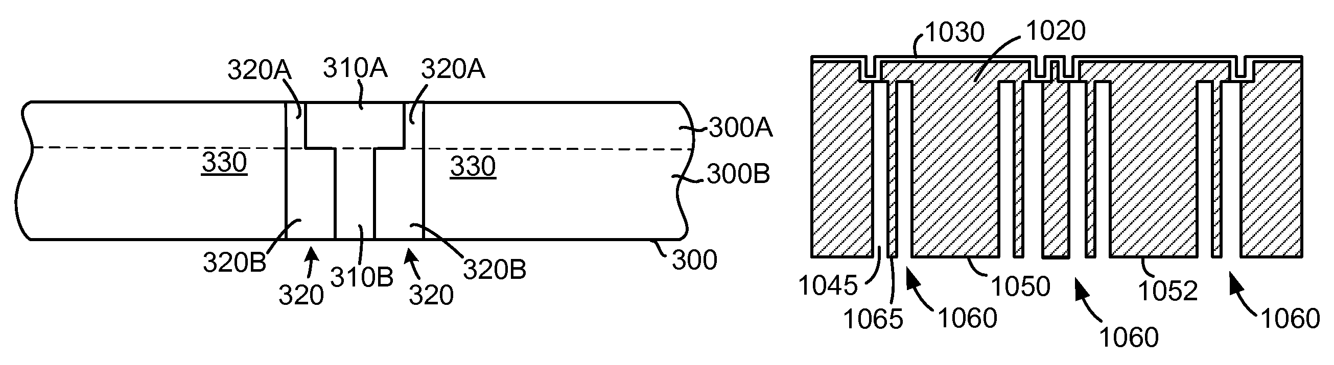
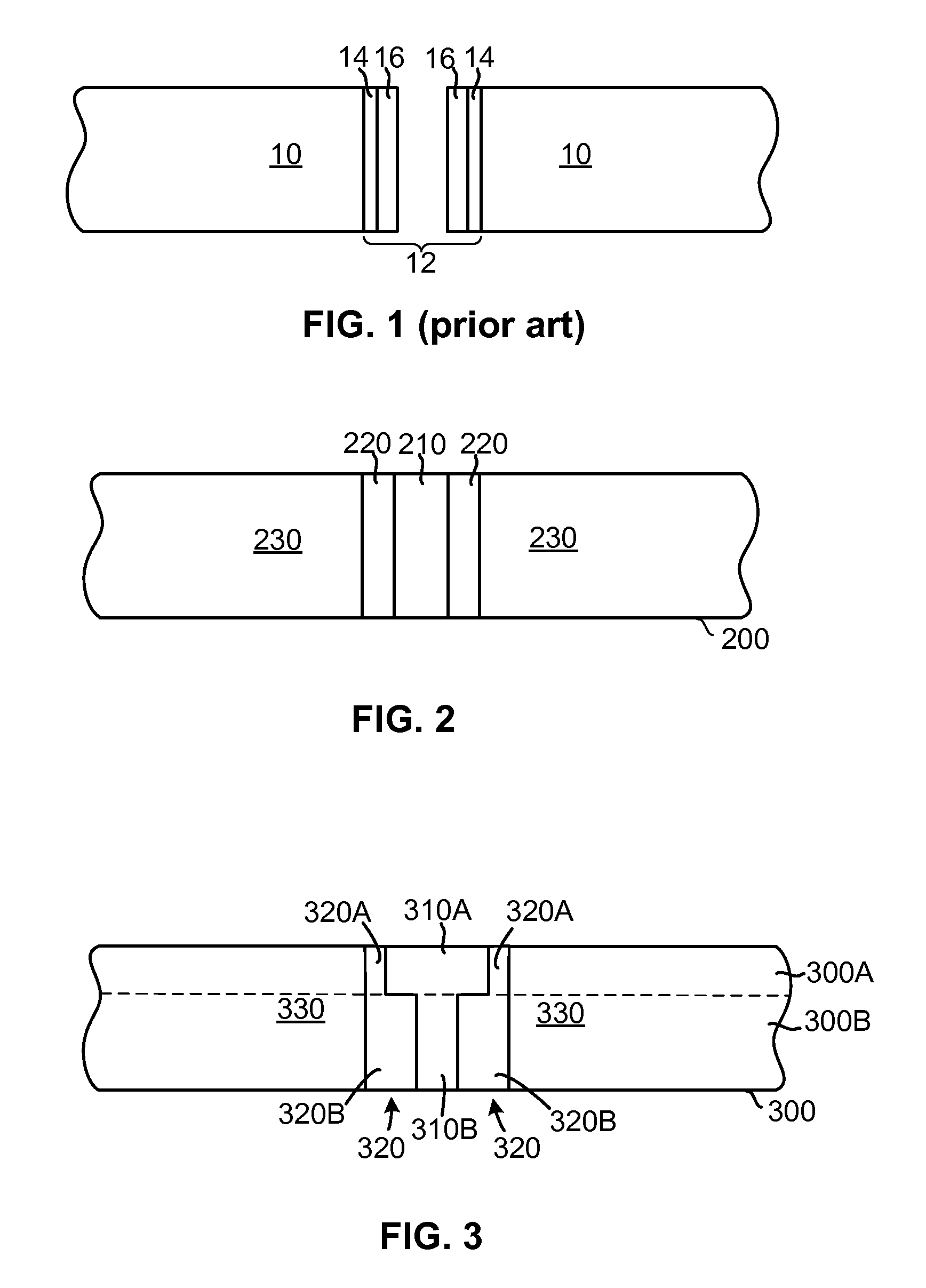
[0058]FIG. 2 is a schematic cross-sectional view of a through-wafer interconnect in accordance with the present invention. The through-wafer interconnect is built in a wafer 200. The through-wafer interconnect includes a conductor 210 passing through the front side (top) of the wafer 200 to the backside (bottom) of the wafer. The conductor 210 is surrounded by an insulator 220, and both the conductor 210 and the insulato...


PUM


Abstract

A through-wafer interconnect and a method for fabricating the same are disclosed. The method starts with a conductive wafer to form a patterned trench by removing material of the conductive wafer. The patterned trench extends in depth from the front side to the backside of the wafer, and has an annular opening generally dividing the conductive wafer into an inner portion and an outer portion whereby the inner portion of the conductive wafer is insulated from the outer portion and serves as a through-wafer conductor. A dielectric material is formed or added into the patterned trench mechanical to support and electrically insulate the through-wafer conductor. Multiple conductors can be formed in an array.

Description

RELATED APPLICATIONS[0001]This application is a national stage application of international application PCT / IB2006 / 051566, claiming priority from U.S. Provisional Application Ser. No. 60 / 682,619, filed May 18, 2005.[0002]This application further incorporates herein by reference in entirety the following:[0003]International application PCT / IB2006 / 051567, entitled METHODS FOR FABRICATING MICRO-ELECTRO-MECHANICAL DEVICES, filed on May 18, 2006;[0004]International application PCT / IB2006 / 051568, entitled MICRO-ELECTRO-MECHANICAL TRANSDUCERS, filed on May 18, 2006; and[0005]International application PCT / IB2006 / 051569, entitled MICRO-ELECTRO-MECHANICAL TRANSDUCERS, filed on May 18, 2006.FIELD OF THE INVENTION[0006]The present invention relates to microelectronics fabrication, and more particularly to through-wafer interconnection in microelectronics fabrication.BACKGROUND OF THE INVENTION[0007]Through-wafer interconnection is a structure that electrically connects devices (e.g. integrate c...

Claims


Application Information

Patent Timeline
Patent Type & Authority Patents(United States)
IPC IPC(8): H01L21/4763
CPCH01L21/76898H01L23/481H01L2924/3011H01L2924/0002H01L2924/00H01L2924/00012
Inventor HUANG, YONGLI
Owner KOLO MEDICAL (SUZHOU) CO LTD
Why Eureka
Try Eureka