Semiconductor apparatus and manufacturing method thereof

a technology of semiconductor devices and manufacturing methods, applied in the direction of electrical devices, semiconductor devices, semiconductor/solid-state device details, etc., can solve the problems of insufficient ashing treatment and difficulty in adopting a technique for improving adhesion properties by ashing treatment, and achieve the effect of improving adhesion properties and reliability

Active Publication Date: 2012-01-31
SHINKO ELECTRIC IND CO LTD
View PDF11 Cites 48 Cited by
  • Summary
  • Abstract
  • Description
  • Claims
  • Application Information

AI Technical Summary

Benefits of technology

[0012]Exemplary embodiments of the present invention provide a semiconductor apparatus capable of obtaining sufficient reliability by improving adhesion properties in a semiconductor apparatus of a structure in which a thinned semiconductor chip is mounted between wiring substrates and is sealed with a resin, and a manufacturing method of the semiconductor apparatus.
[0024]Therefore, even when moisture absorbed by the semiconductor apparatus vaporizes and volume expansion is caused, an interface of the upper surface side of the semiconductor chip has sufficient adhesion properties, so that peeling is prevented from occurring at their interfaces. Consequently, reliability of the semiconductor apparatus can be improved.
[0025]As mentioned above, in the present invention, it is possible to obtain sufficient reliability by improving adhesion properties in a semiconductor apparatus of a structure in which a thinned semiconductor chip is mounted between wiring substrates and is sealed with a resin.

Problems solved by technology

However, in the related art, the second wiring substrate 400 is present on the semiconductor chip 200, so that the ashing treatment cannot be performed sufficiently with respect to the upper surface of the semiconductor chip 200 and it is difficult to adopt a technique for improving adhesion properties by the ashing treatment.

Method used


Image

  • Semiconductor apparatus and manufacturing method thereof
  • Semiconductor apparatus and manufacturing method thereof
  • Semiconductor apparatus and manufacturing method thereof

Examples


first embodiment

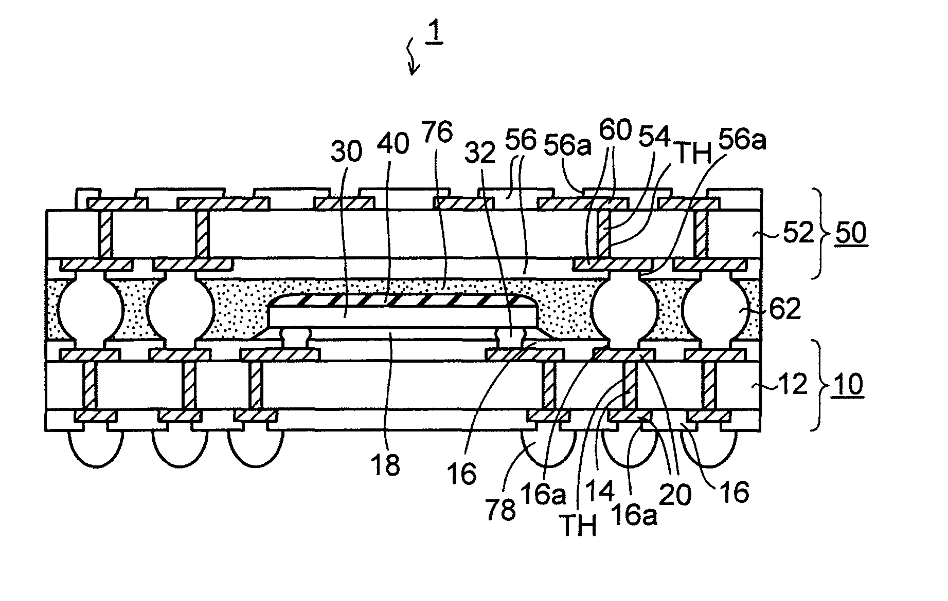
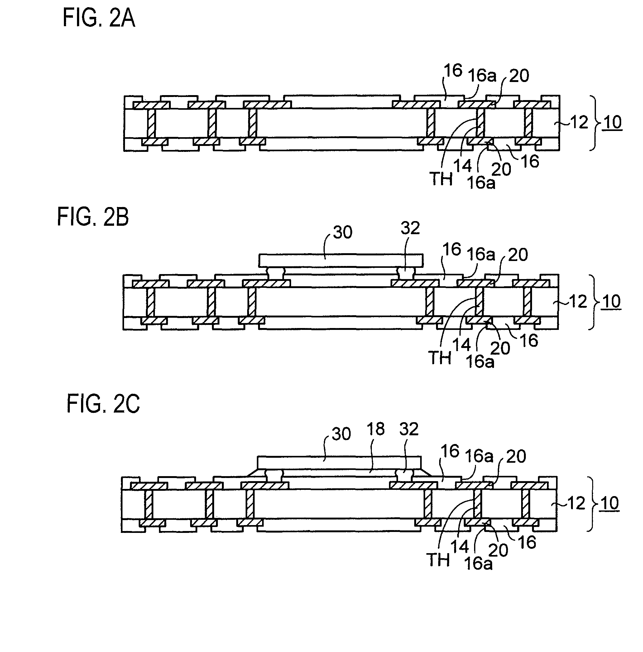
[0045]FIGS. 2 to 5 are sectional views showing a manufacturing method of a semiconductor apparatus of a first embodiment of the invention. In the manufacturing method of the semiconductor apparatus of the first embodiment, a first wiring substrate 10 as shown in FIG. 2A is first prepared. In the first wiring substrate 10, a through hole TH is disposed in a core substrate 12 made of an insulating material such as a glass epoxy resin. Wiring layers 20 mutually connected through a through electrode 14 with which the inside of the through hole TH is filled are respectively formed on the sides of both surfaces of the core substrate 12.

[0046]Or, the wiring layers 20 may be mutually connected through a through hole plated layer (through electrode) disposed on an inner wall of the through hole TH of the core substrate 12 and a hole of the through hole TH may be filled with a resin.

[0047]Further, solder resists 16 in which opening parts 16a are disposed on connection parts of the wiring laye...

second embodiment

[0087]FIGS. 6 and 7 are sectional views showing a manufacturing method of a semiconductor apparatus of a second embodiment of the invention.

[0088]The second embodiment is characterized in that a semiconductor chip is made to adhere to a second wiring substrate directly by an adhesive layer without interposing a molding resin between an upper surface (mirror surface) of the semiconductor chip and a lower surface of the second wiring substrate.

[0089]In the second embodiment, the detailed description is omitted by assigning the same numerals to the same elements and the same steps as those of the first embodiment.

[0090]In the manufacturing method of the semiconductor apparatus of the second embodiment, the same structural body as that of FIG. 2C of the first embodiment described above is prepared as shown in FIG. 6A. That is, after a semiconductor chip 30 is mounted in a first wiring substrate 10 by flip chip bonding, a gap between a lower portion of the semiconductor chip 30 and an up...


PUM


Abstract

A semiconductor apparatus includes a first wiring substrate, a second wiring substrate, a semiconductor chip, an adhesive layer and a molding resin. The second wiring substrate is stacked and connected on the first wiring substrate through a bump electrode. The semiconductor chip is mounted on the first wiring substrate by flip chip bonding and received between the first wiring substrate and the second wiring substrate. An upper surface of the semiconductor chip is subject to a mirror treatment. The adhesive layer is formed on the upper surface of the semiconductor chip. The molding resin is filled in a gap between the first wiring substrate and the second wiring substrate.

Description

[0001]This application claims priority to Japanese Patent Application No. 2008-321038, filed Dec. 17, 2008, in the Japanese Patent Office. The Japanese Patent Application No. 2008-321038 is incorporated by reference in its entirety.TECHNICAL FIELD[0002]The present disclosure relates to a semiconductor apparatus and a manufacturing method thereof, and more particularly to a resin-sealed semiconductor apparatus in which a semiconductor chip is received between stacked wiring substrates and a gap between the wiring substrates is filled with a resin, and a manufacturing method of the semiconductor apparatus.RELATED ART[0003]There are various semiconductor apparatuses. Description in which plural substrates, on each of which an electronic component is mounted, are stacked on a substrate, on which an electronic component is mounted through a solder ball, and a gap between the substrates is sealed with a resin is made in Patent Reference 1.[0004]Also, description in which one wiring substr...

Claims


Application Information

Patent Timeline
Patent Type & Authority Patents(United States)
IPC IPC(8): H01L23/02H01L21/50
CPCH01L21/565H01L23/16H01L23/3128H01L24/73H01L25/105H01L21/563H01L24/16H01L24/29H01L24/32H01L2224/16237H01L2224/73253H01L2924/01013H01L2924/01029H01L2924/01078H01L2924/01079H01L2924/01082H01L2924/01088H01L2924/12044H01L2924/15311H01L2924/15331H01L2924/01005H01L2924/01006H01L2924/01033H01L2224/16225H01L2224/32225H01L2224/73204H01L2225/1023H01L2225/1041H01L2225/1058H01L2924/3512H01L2924/00H01L2224/92125H01L2924/00012H01L2924/181H01L2924/00014H01L2224/0401H01L2924/00011
Inventor KAJIKI, ATSUNORI
Owner SHINKO ELECTRIC IND CO LTD
Why Eureka
Try Eureka