Multi-layered device and electronic equipment using thereof

a multi-layer device and electronic equipment technology, applied in the direction of multiple-port networks, electrical devices, impedence networks, etc., can solve the problems of large insertion loss, weak magnetic coupling, and inability to obtain desired characteristics, so as to suppress the magnetic coupling and shorten the length of the first viahole inductor conductor

Inactive Publication Date: 2012-01-31
PANASONIC CORP
View PDF6 Cites 11 Cited by
  • Summary
  • Abstract
  • Description
  • Claims
  • Application Information

AI Technical Summary

Benefits of technology

[0014]In view of the above mentioned circumstances, it is an object of the present invention to suppress the deterioration in the characteristics of a multi-layered device including a plurality of resonators.
[0016]According to the multi-layered device according to the present invention, the length of the first viahole inductor conductor can be shortened by providing the inductor electrode layer arranged substantially in parallel to the dielectric sheet layer, and, as a result, it is possible to suppress the magnetic coupling between the first and second viahole inductor conductors.

Problems solved by technology

However, the above-mentioned multi-layered device according to the prior art has such a problem that the reduction in the height of the multi-layered device results in a large insertion loss, and desired characteristics cannot be obtained when the multi-layered device is made smaller, since the magnetic coupling between the resonators becomes too strong due to a narrowed interval between the resonators.
Namely, there is such a problem that the magnetic coupling becomes strong particularly when a distance between the first and second viahole inductor conductors is shorter than 1.5 times the length of the first viahole inductor conductor.
Conversely, when it is tried to secure a sufficient attenuation in this frequency range, the characteristics in the passband is significantly deformed, and the insertion loss becomes larger than 3 dB.
In addition, the impedance matching is also worsened, and this leads to degraded usability as a filter.
As described above, the narrowed interval between the resonators inevitably causes the stronger magnetic coupling and deterioration in the performance, and this leads to a serious hindrance to promoting the size reduction.

Method used


Image

  • Multi-layered device and electronic equipment using thereof
  • Multi-layered device and electronic equipment using thereof
  • Multi-layered device and electronic equipment using thereof

Examples


first preferred embodiment

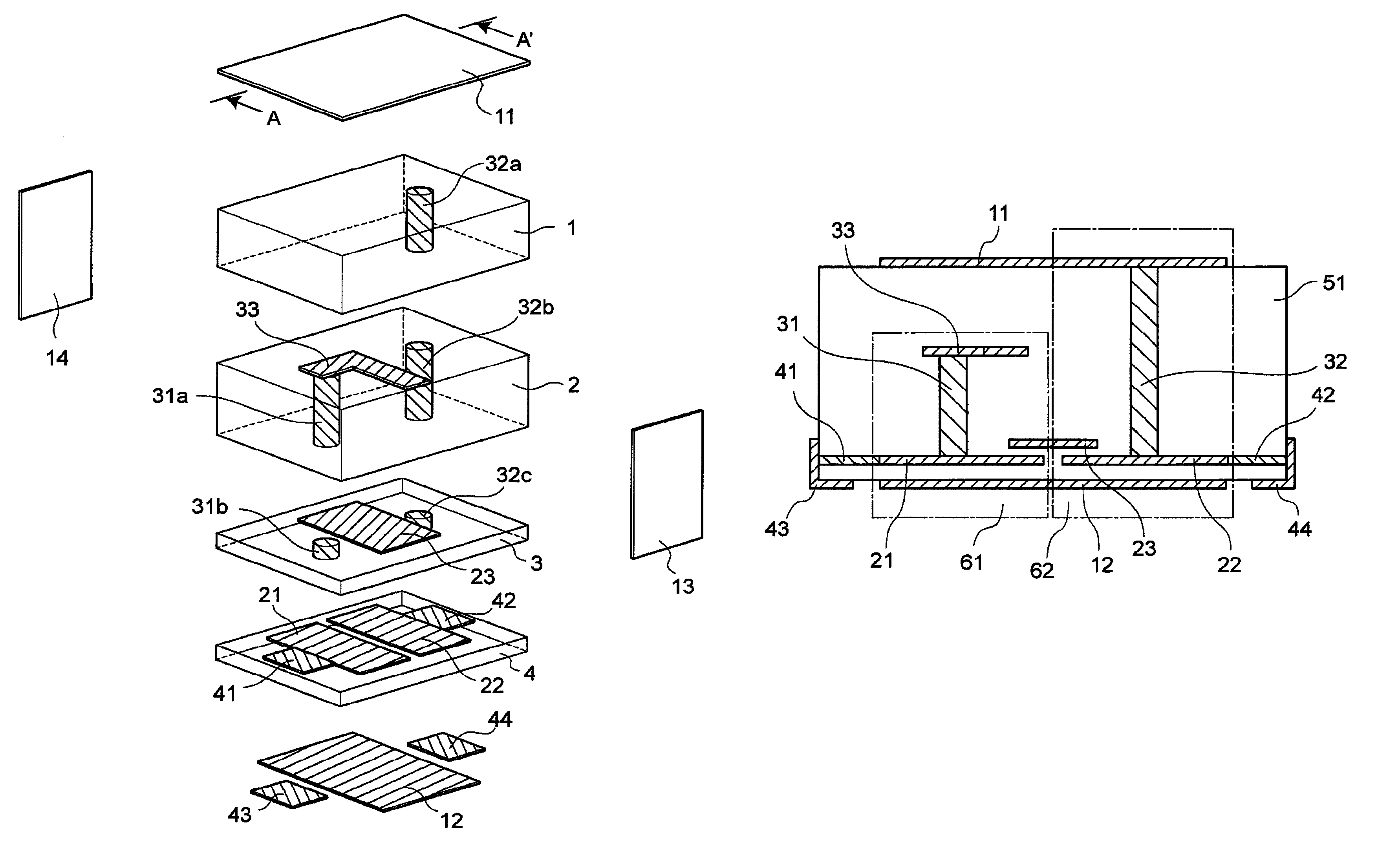
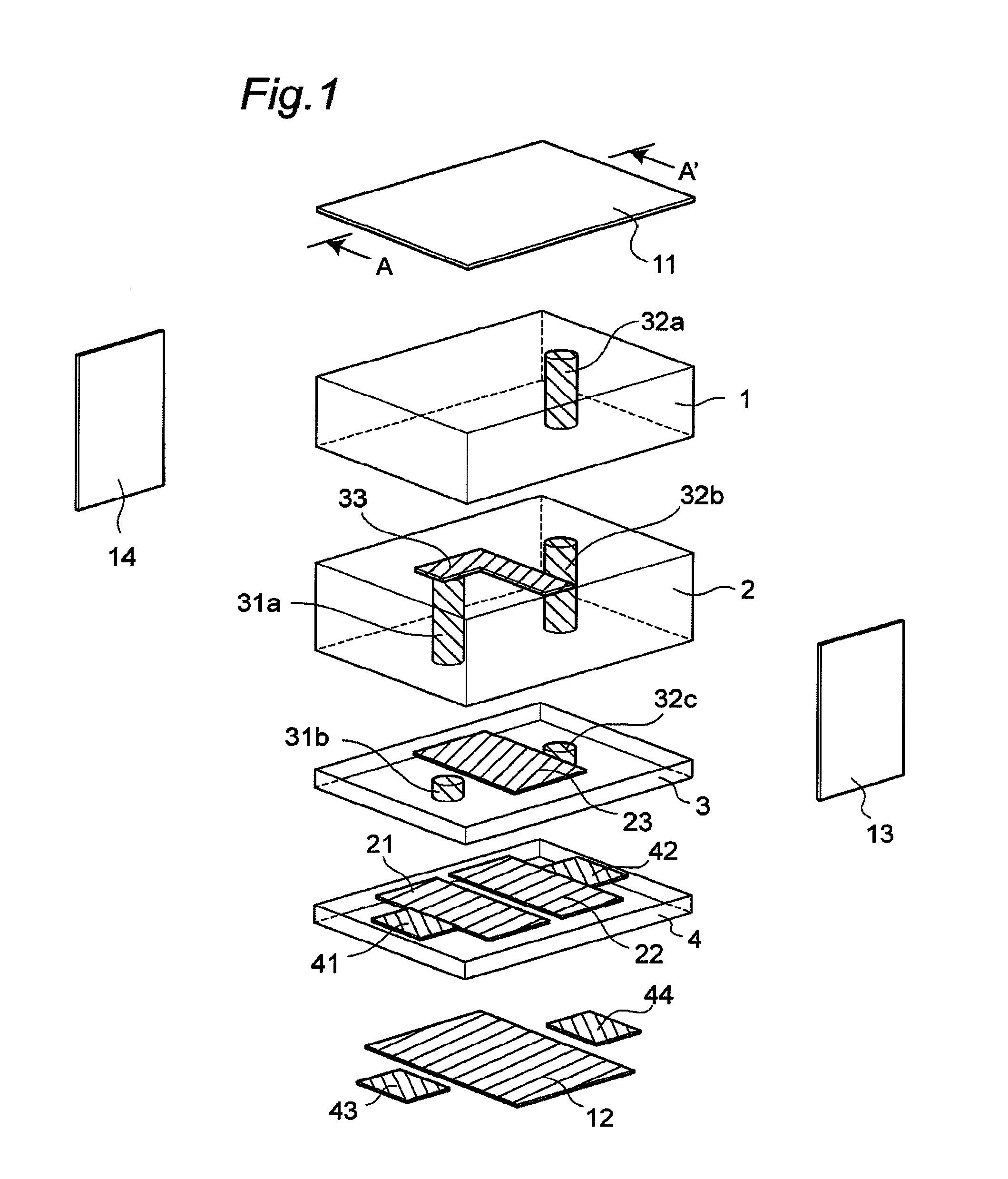
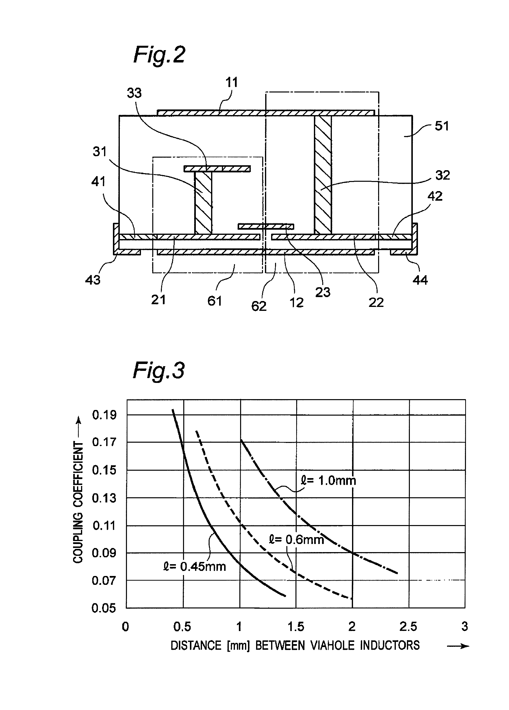
[0032]A multi-layered device according to a first preferred embodiment will be described below with reference to FIGS. 1 and 2. FIG. 1 is an exploded perspective view of the multi-layered device according to the first preferred embodiment of the present invention. In addition, FIG. 2 is a sectional schematic view (a sectional view along a line A-A′ of FIG. 1) of the multi-layered device according to the first preferred embodiment.

[0033]The multi-layered device according to the first preferred embodiment includes an insulator 51 including a plurality of multi-layered dielectric sheet layers 1, 2, 3 and 4, ground electrode layers 11 and 12 arranged substantially in parallel to the dielectric sheet layer 1, inside or on the surfaces of the insulator 51, side-surface ground electrodes 13 and 14 arranged on mutually opposite side surfaces of the insulator 51, and a plurality of resonators 61 and 62 formed in the insulator 51. The first resonator 61, which is one of the plurality of reson...


PUM


Abstract

A multi-layered device includes an inductor electrode layer connected between one end of a first viahole inductor conductor and a side-surface ground electrode, and arranged substantially in parallel to a dielectric sheet, when the first and second viahole inductor conductors are arranged in such a positional relation that a distance between the first and second viahole inductor conductors is smaller than 1.5 times a length of the first viahole inductor conductor.

Description

BACKGROUND OF THE INVENTION[0001]1. Field of the Invention[0002]The present invention relates to a multi-layered device including a plurality of multi-layered insulator layers, and an electronic equipment that employs the multi-layered device.[0003]2. Description of the Related Art[0004]Conventionally, there have been proposed various multi-layered devices including multi-layered ceramic insulators and a plurality of resonators built in the layered ceramic insulators. Referring to FIGS. 9 and 10, a multi-layered device according to a prior art will be described below. FIG. 9 is an exploded perspective view of the multi-layered device according to the prior art. In addition, FIG. 10 is a sectional schematic view (a sectional view along a line B-B′ of FIG. 9) of the multi-layered device according to the prior art. It is noted that the common components are denoted by the same reference numerals.[0005]Referring to FIGS. 9 and 10, reference numerals 901, 902, 903, 904 and 905 denote die...

Claims


Application Information

Patent Timeline
Patent Type & Authority Patents(United States)
IPC IPC(8): H01H7/00
CPCH03H7/01H03H7/09H03H2001/0085
Inventor SHIMAMURA, TETSUROHOEFT, MICHAEL
Owner PANASONIC CORP
Why Eureka
Try Eureka