

Luminescent device and method of manufacturing the same
A technology for a light-emitting device and a manufacturing method, which is applied to semiconductor devices, electrical solid-state devices, electrical components, etc., can solve the problems of reduced adhesion or sealing performance of joints, high manufacturing costs, and many manufacturing processes, and achieves reliability. , Simple manufacturing method, the effect of reducing the manufacturing process
- Summary
- Abstract
- Description
- Claims
- Application Information
AI Technical Summary
Problems solved by technology
Method used
Image

Examples
Embodiment 1
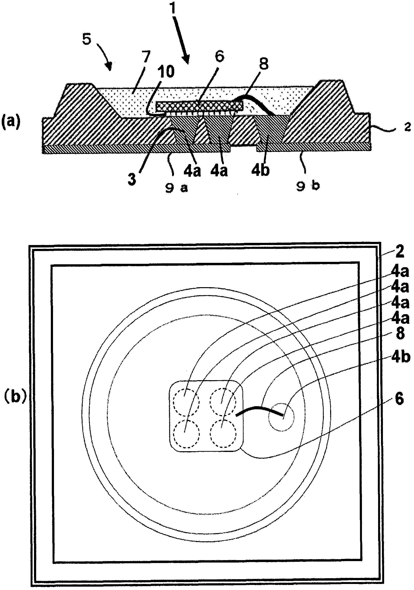
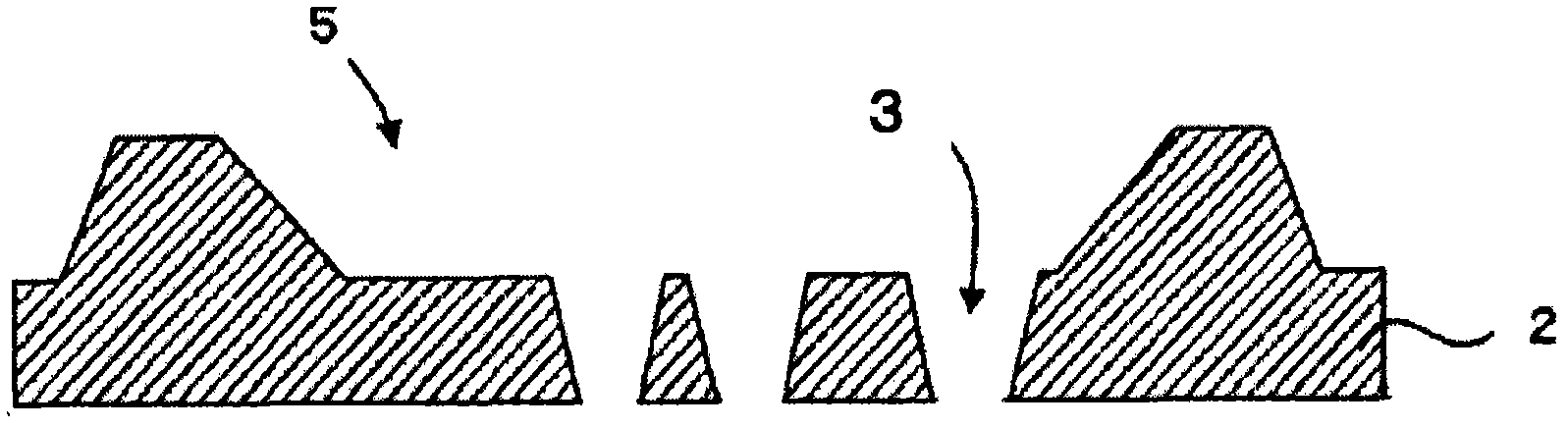
[0033] figure 1 The structure of the light emitting device according to this embodiment is schematically shown. figure 1 (a) is a cross-sectional view of the light emitting device, figure 1(b) is its plan view. The glass substrate 2 is in the shape of a substantially rectangular thin plate, and a substantially truncated cone-shaped depression 5 whose diameter gradually decreases from top to bottom is formed in the center thereof. Alternatively, an inner-inclined protrusion is provided on the outer peripheral portion of the glass substrate 2 , and the area surrounded by the protrusion can be regarded as the depression 5 . A plurality of through-holes 3 are formed on the glass surface of the pit 5 . The through hole 3 has a cross-sectional shape expanding from the back surface of the glass substrate 2 toward the glass surface of the recess 5 . Electrodes (not shown) are formed on the upper surface and the lower surface of the LED element 6 . The lower surface electrode i...
Embodiment 2
[0052] Figure 5 is a cross-sectional view schematically showing the light-emitting device 1 of this embodiment. In addition, descriptions that overlap with Example 1 are appropriately omitted. As shown in the figure, in this embodiment, a structure in which the glass lens 21 is integrated with the light emitting device of Embodiment 1 is adopted. The glass substrate 2 and the glass lens 21 are bonded together by the adhesive 22 coated on the top surface of the protrusion 23 of the glass substrate 2 . As shown in the figure, when the amount of the sealant 7 supplied to the recess of the glass substrate 2 is small, a gap may exist between the sealant 7 and the glass lens 21 .
[0053] According to this structure, since the light-emitting element 6 is completely sealed by the glass substrate and the glass lens, a highly durable light-emitting device can be realized. Here, a hemispherical convex lens is used, but an elliptical or concave lens may be used, or a different shape ...
Embodiment 3
[0057] Next, an embodiment in which the bottom surface of the glass lens 21 is not flat will be described with reference to the drawings. Here, "the bottom surface of the glass lens 21" refers to the surface (installation surface) on the side connected to the glass base. In addition, descriptions that overlap with Embodiment 2 are appropriately omitted.
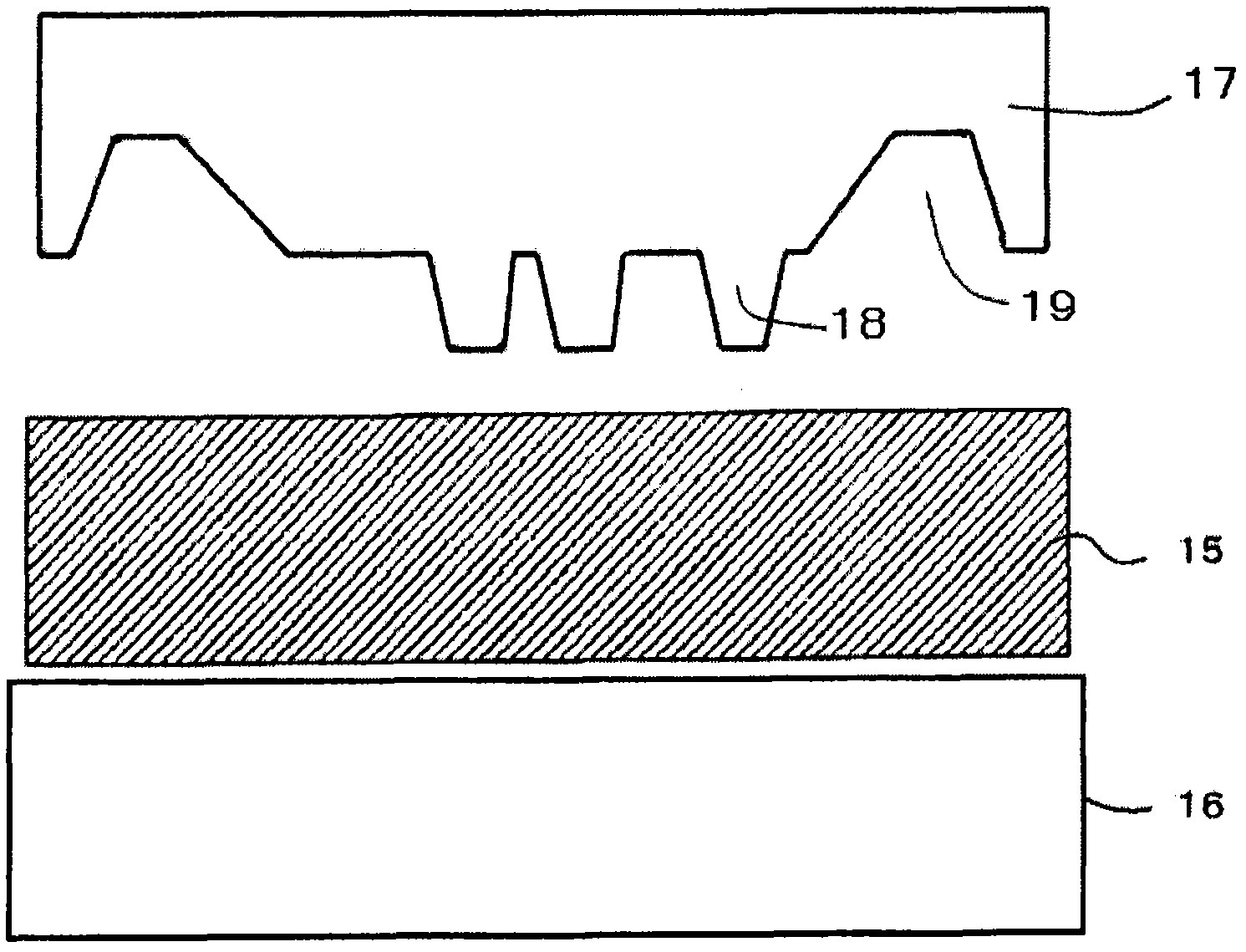
[0058] Figure 7 A cross-sectional structure of a light emitting device in which a convex portion 24 is provided on the bottom surface of a glass lens 21 is schematically shown. As shown in the figure, the convex portion 24 of the glass lens 21 is closely fitted to the upper portion of the inclined surface of the recess of the glass base 2 (the upper portion of the inner wall surface of the protrusion 23 of the glass base 2 ). In this way, the glass substrate 2 and the glass lens 21 can be aligned with high precision by arranging the outer peripheral slope of the convex portion 24 of the glass lens 21 in contact with the sl...
PUM
 Abstract
Description
Claims
Application Information