Radio frequency module

a technology of radio frequency and module, which is applied in the direction of gated amplifier, semiconductor/solid-state device details, transmission, etc., can solve the problems of reducing the characteristics of the amplifier circuit, affecting the rf signal processing, and generating capacitance, etc., to achieve increased cross-sectional area, increase mounting strength, and large area

Active Publication Date: 2020-01-02
MURATA MFG CO LTD
View PDF0 Cites 8 Cited by
  • Summary
  • Abstract
  • Description
  • Claims
  • Application Information

AI Technical Summary

Benefits of technology

[0029]In this manner, by increasing the cross-sectional area of the leading-end portion of the bump electrode, a large area can be used to connect to a motherboard in a case where the RF module is mounted on the motherboard, thereby increasing the mounting strength.
[0030]In an RF module, degradation of the characteristics of an amplifier circuit due to a generated parasitic capacitance is suppressed.

Problems solved by technology

However, in the RF module described in Patent Document 1, there may be a case where, depending on the design of a wire between the integrated circuit device and the inductor device, a parasitic capacitance may be generated between this wire and another wire and the RF signal processing may be adversely affected.
In particular, in a case where the integrated circuit device includes an amplifier circuit, there is a problem in that the generation of a parasitic capacitance degrades the characteristics of the amplifier circuit.

Method used


Image

  • Radio frequency module
  • Radio frequency module
  • Radio frequency module

Examples


first embodiment

1-1. Configuration of RF Module

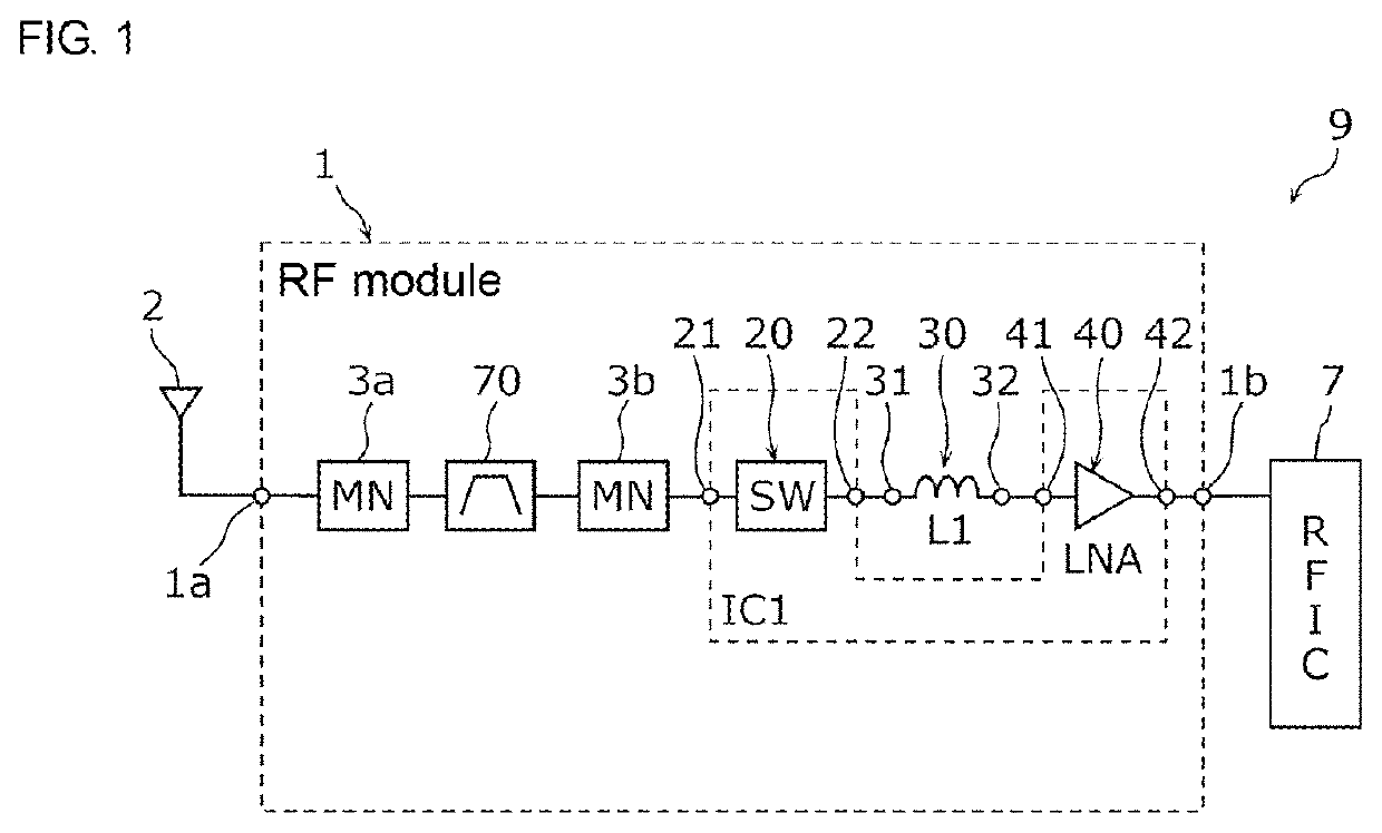
[0039]First, a circuit configuration of an RF module 1 according to a first embodiment will be described.

[0040]FIG. 1 is a diagram illustrating the circuit configuration of the RF module 1.

[0041]The RF module 1 is a circuit module that amplifies and transfers RF signals. An antenna element 2 is connected to an antenna terminal 1a of the RF module 1, and a radio frequency integrated circuit (RFIC) 7, which is an RF signal processing circuit, is connected to an input-output terminal 1b. Note that FIG. 1 illustrates a communication device 9 including the RF module 1 and the RFIC 7. In the present embodiment, a description will be made taking the RF module 1, which is a receiving circuit, as an example.

[0042]In the RF module 1, a matching element (MN) 3a, a band pass filter 70, a matching element (MN) 3b, a switch circuit unit 20, a matching circuit unit 30, an amplifier circuit unit 40, and the input-output terminal 1b are arranged in this order from the ...

second embodiment

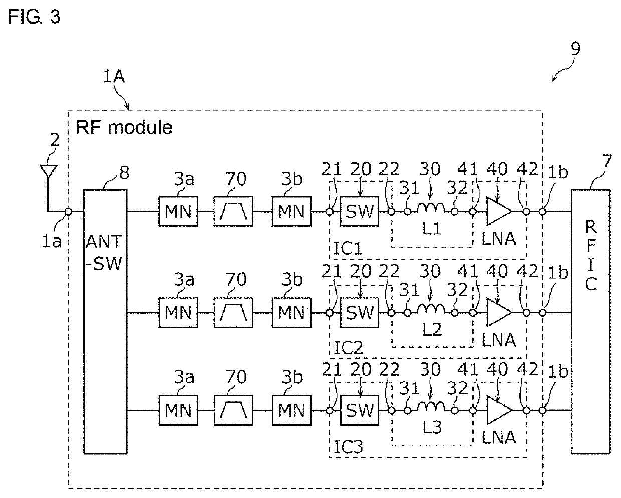
[0073]Next, an RF module 1A according to a second embodiment will be described. The RF module 1A according to the second embodiment has three RF signal channels.

[0074]FIG. 3 is a diagram illustrating the circuit configuration of the RF module 1A.

[0075]As illustrated in FIG. 3, the RF module 1A has the antenna terminal 1a and three input-output terminals 1b. The antenna element 2 is connected to the antenna terminal 1a, and the RFIC 7 is connected to the three input-output terminals 1b.

[0076]The RF module 1A has an antenna switch 8 and the three RF signal channels in the channel connecting the antenna terminal 1a to the input-output terminals 1b. The antenna switch 8 has one common terminal and three selection terminals. Each RF signal channel has the matching element (MN) 3a, the band pass filter 70, the matching element (MN) 3b, the switch circuit unit 20, the matching circuit unit 30, and the amplifier circuit unit 40. In the present embodiment, the integrated circuit device IC1 ...

third embodiment

[0089]Next, an RF module 1B according to a third embodiment will be described. In the RF module 1B according to the third embodiment, a bottom portion 81 of a bump electrode 80 is thick and the bottom portion 81 is connected to the second shield film 62.

[0090]FIG. 5 is a cross section of the RF module 1B when the RF module 1B is viewed from the front.

[0091]As illustrated in FIG. 5, the RF module 1B includes the substrate 10, the matching circuit unit 30 mounted on the one main surface 10a of the substrate 10, and the integrated circuit device IC1 mounted on the other main surface 10b. A plurality of mount components 75 are joined to the one main surface 10a of the substrate 10 using a joining member 76 such as solder.

[0092]The RF module 1B has a plurality of bump electrodes 80, and some of the bump electrodes 80 are electrodes connected to the ground. As illustrated in FIG. 5, each bump electrode 80 connected to the ground has the bottom portion 81, which is in contact with the othe...


PUM


Abstract

An amplifier circuit unit of a radio frequency module is mounted on a substrate with a first external terminal interposed therebetween, a switch circuit unit is mounted on the substrate with a second external terminal interposed therebetween, and a matching circuit unit is mounted on the substrate with a first terminal and a second terminal interposed therebetween. The first terminal is electrically connected to the second external terminal of the switch circuit unit, and the second terminal is electrically connected to the first external terminal of the amplifier circuit unit. When viewed from a direction perpendicular to one main surface of the substrate, the first terminal is superposed with the second external terminal of the switch circuit unit, and the second terminal is superposed with the first external terminal of the amplifier circuit unit.

Description

[0001]This is a continuation of International Application No. PCT / JP2018 / 009052 filed on Mar. 8, 2018 which claims priority from Japanese Patent Application No. 2017-048707 filed on Mar. 14, 2017. The contents of these applications are incorporated herein by reference in their entireties.BACKGROUNDTechnical Field[0002]The present disclosure relates to a radio frequency (RF) module that amplifies and transfers radio frequency (RF) signals.[0003]In recent years, higher-density integration has been achieved for, for example, a switch circuit component and an amplifier circuit component that are components included in an RF module. As higher-density integration has been achieved for these components, wiring for connecting the components and wiring for connecting the components to a matching element have become more complicated.[0004]As an example of this type of RF module, Patent Document 1 describes an RF module including an integrated circuit device built in a substrate and an inducto...

Claims


Application Information

Patent Timeline
Patent Type & Authority Applications(United States)
IPC IPC(8): H04B1/04H03F3/195H03F3/24H04B1/00
CPCH03F3/245H03F2200/451H04B2001/0408H03F3/195H04B1/0042H04B1/04H01L23/12H01L25/00H04B1/18H03F2200/111H03F3/72H03F2203/7209
Inventor WATANABE, TAKASHI
Owner MURATA MFG CO LTD
Why Eureka
Try Eureka