

Dual polarized waveguide feed arrangement with symmetrically tapered structures
a technology of symmetric tapered structure and waveguide, which is applied in the direction of waveguides, electrical equipment, multiple-port networks, etc., can solve the problems of affecting the cost negatively, the dual polarized feeding arrangement of today becomes very expensive, etc., and achieves the effect of being less costly and simpl
- Summary
- Abstract
- Description
- Claims
- Application Information
AI Technical Summary
Benefits of technology
Problems solved by technology
Method used
Image

Examples
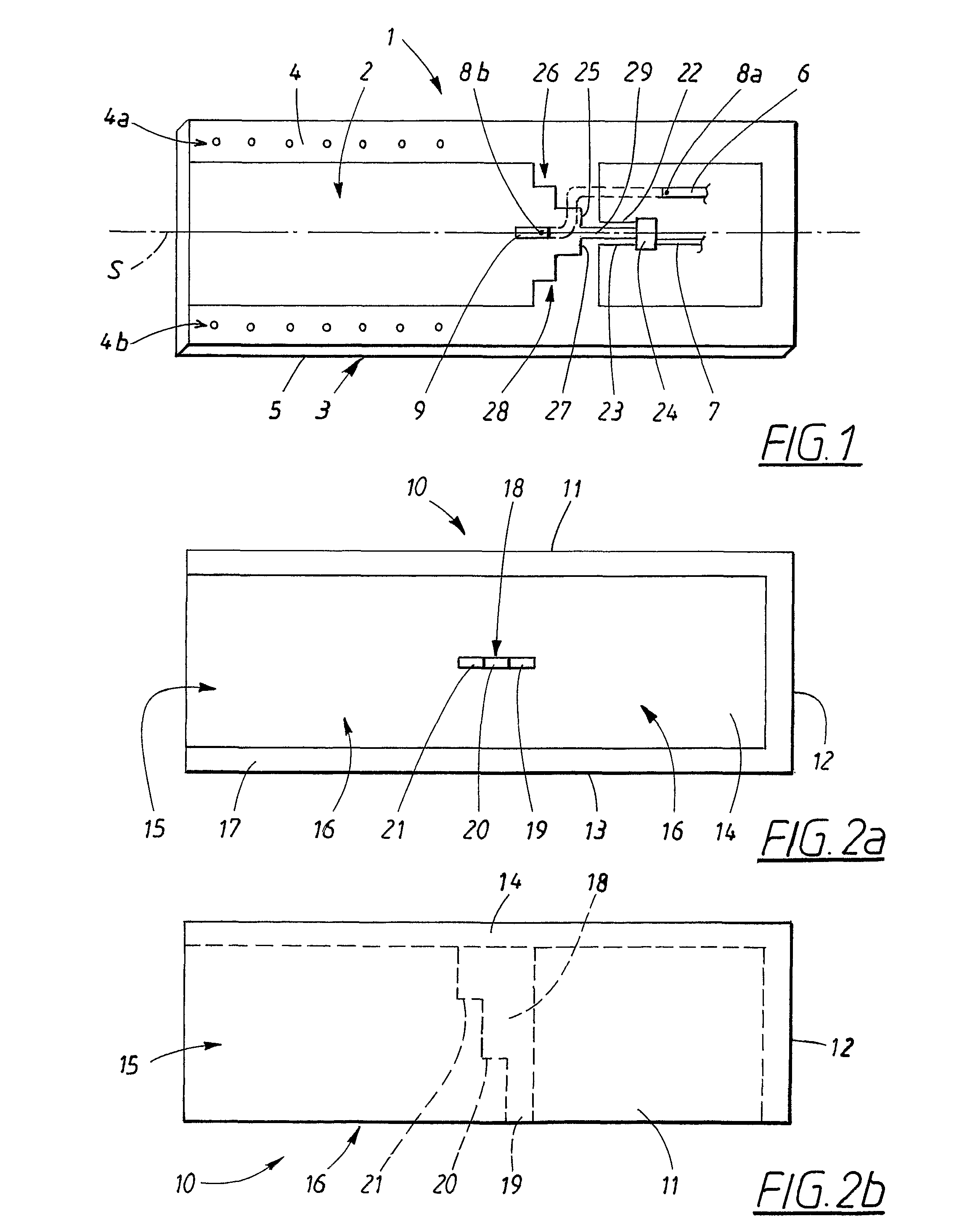
first embodiment
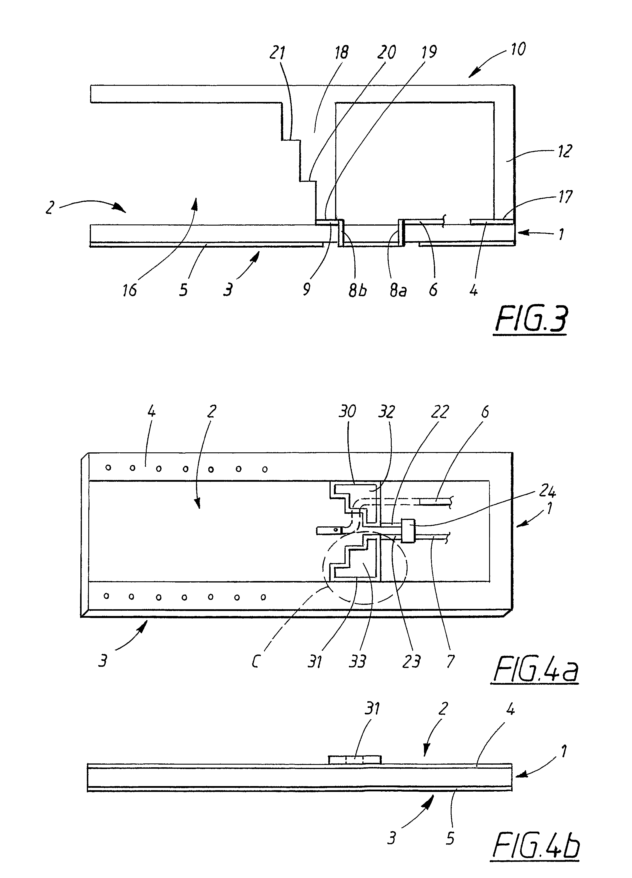
[0054]In a second preferred embodiment, with reference to FIG. 4a and FIG. 4b, where FIG. 4b shows a side view of the top view in FIG. 4a, a first closed wall structure 30 (FIG. 4) and a second closed wall structure 31 is mounted on the dielectric carrier material 1, the walls extending perpendicular to the first main side 2. Each wall structure 30, 31 has an outer contour which corresponds to the outer contour of the etched ridge structures 26, 28 in FIG. 1. Each wall structure 30, 31 is soldered to the respective feeding sub-conductors 22, 23 (FIG. 4), such that the wall structures 30, 31 are fed in a similar way as the etched ridge structures, via the second feeding conductor 7 and the combined power divider and 180° phase shifter 24. Preferably, the wall structures 30, 31 are secured by means of pins (not shown) that are inserted into corresponding holes in the dielectric carrier material 1 and soldered. The walls have a certain height and a certain width, surrounding a respect...
second embodiment
[0060]In the second embodiment varieties as disclosed above with reference to the FIGS. 4a-4f, the etched ridge structure may be present on the dielectric carrier when the waveguide part is mounted to the dielectric carrier.
[0061]A third embodiment is shown in FIG. 5a, where the etched ridge structures according to the first embodiment are utilized. The dielectric carrier material 1′ is in the form of a multilayer carrier, comprising a first main side 2′ (FIG. 5a) and a second main side 3′ (FIG. 5a) as described for the first embodiment. Here, the first main side 2′ is positioned on the outwardly facing side of a first dielectric layer 39, and the second main side 3′ is positioned on the outwardly facing side of a second dielectric layer 40. Sandwiched between the first dielectric layer 39 and the second dielectric layer 40 there is an intermediate metalization 41, being of the same kind as the metalization on the first 2′ and second 3′ main sides. The intermediate metalization 41 (...
fourth embodiment
[0077]A special variety of the fourth embodiment is shown in FIG. 7a, where a first waveguide part 57a and a second waveguide part 57b are formed integrally, constituting an integral waveguide part 58. The integral waveguide part 58 has a first side 59, a second side 60, a third side 61 and a fourth side 62. The first side 59 the and third side 61 are opposite each other, and each one of these sides 59, 61 is supplied with a respective first longitudinal slot 63 and second longitudinal slot 64 (FIG. 7a) formed on the middle of the opposing surfaces 65, 66 of the first side 59 and the third side 61.
[0078]With reference to FIG. 7b, the dielectric carrier material 1″, comprising a suitable number of dielectric layers (not shown), is inserted into these slots 63, 64 to a correct longitudinal position.
[0079]The first contact pad and second contact pad are then soldered to a respective stepped structure 67, 68. In this special variety, the integral waveguide part 58 is not surface-mounted...
PUM
 Abstract
Description
Claims
Application Information