Conductive wire pattern and method of monitoring the bonding error of a film

a technology of conductive wire and film, which is applied in the direction of measurement devices, printed circuits, instruments, etc., can solve the problems of low efficiency and inability to control accuracy, and achieve the effect of increasing efficiency and the accuracy of detecting bonding error of films and low efficiency

Inactive Publication Date: 2012-03-27
CHUNGHWA PICTURE TUBES LTD
View PDF31 Cites 3 Cited by
  • Summary
  • Abstract
  • Description
  • Claims
  • Application Information

AI Technical Summary

Benefits of technology

[0010]One objective of the present invention is to provide a special conductive line pattern of a pad area and a method of utilizing the conductive wire pattern to monitor a bonding error of a film, so that the efficiency and the accuracy of detecting bonding error of a film is increased. The problem of the conventional method of detecting the bonding error of a film includes time consuming with the troublesome procedures, causing low efficiency and not being able to control the accuracy is thus solved.

Problems solved by technology

The problem of the conventional method of detecting the bonding error of a film includes time consuming with the troublesome procedures, causing low efficiency and not being able to control the accuracy is thus solved.

Method used


Image

  • Conductive wire pattern and method of monitoring the bonding error of a film
  • Conductive wire pattern and method of monitoring the bonding error of a film
  • Conductive wire pattern and method of monitoring the bonding error of a film

Examples


Embodiment Construction

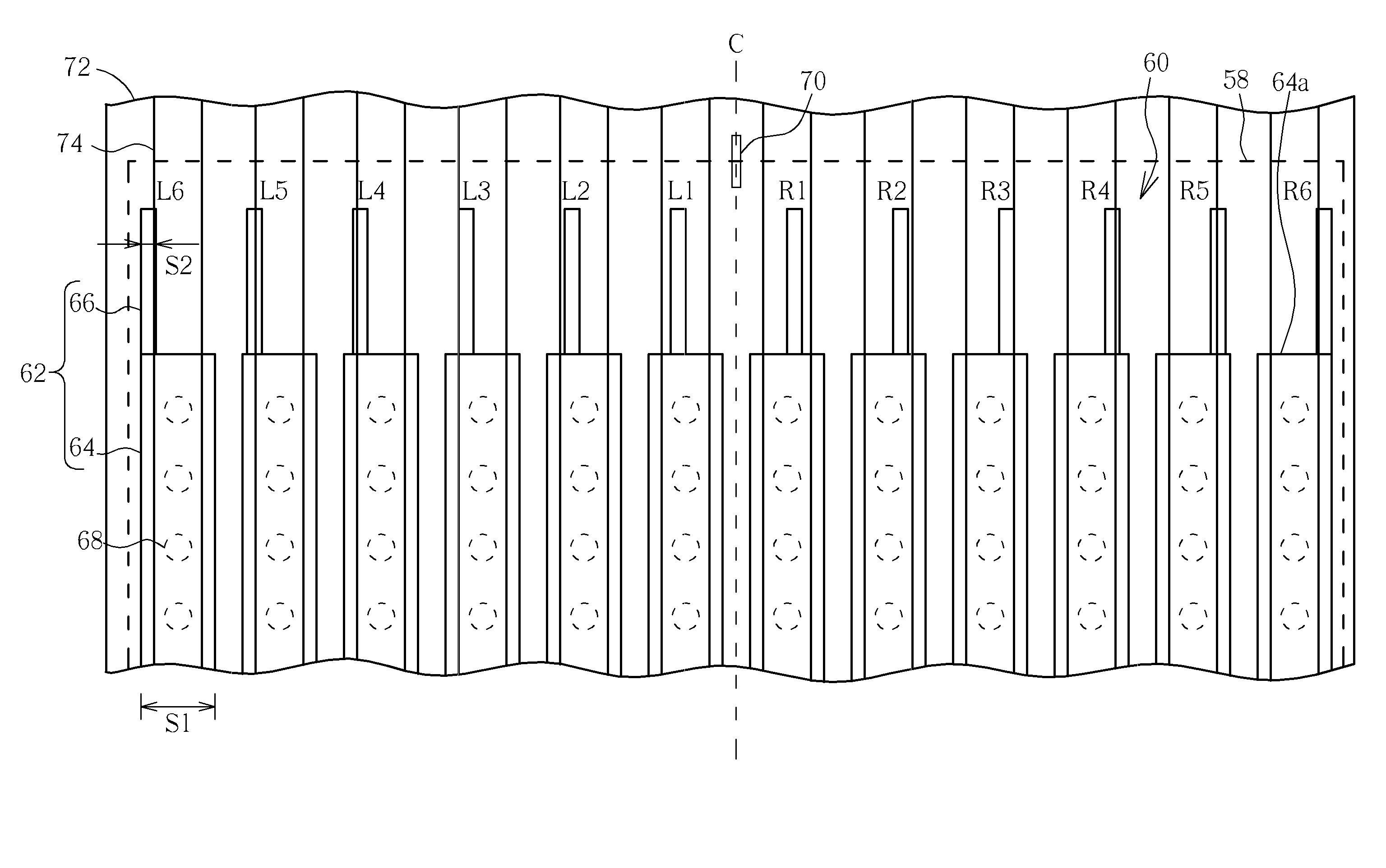
[0024]Please refer to FIG. 7. FIG. 7 is a schematic diagram of a conductive wire pattern in application of an LCD panel of the present invention. An LCD panel 50 includes an array substrate 52 and a CF substrate 54. The region of the array substrate 52 that is not covered by the CF substrate 54 is defined as a non-display region 56. A plurality of pad areas 58 are disposed in the non-display region 56 (only the pad areas of the signal lines are shown in FIG. 7), for disposing terminals so as to electrically connect to the outer circuit and drive the LCD panel 50.

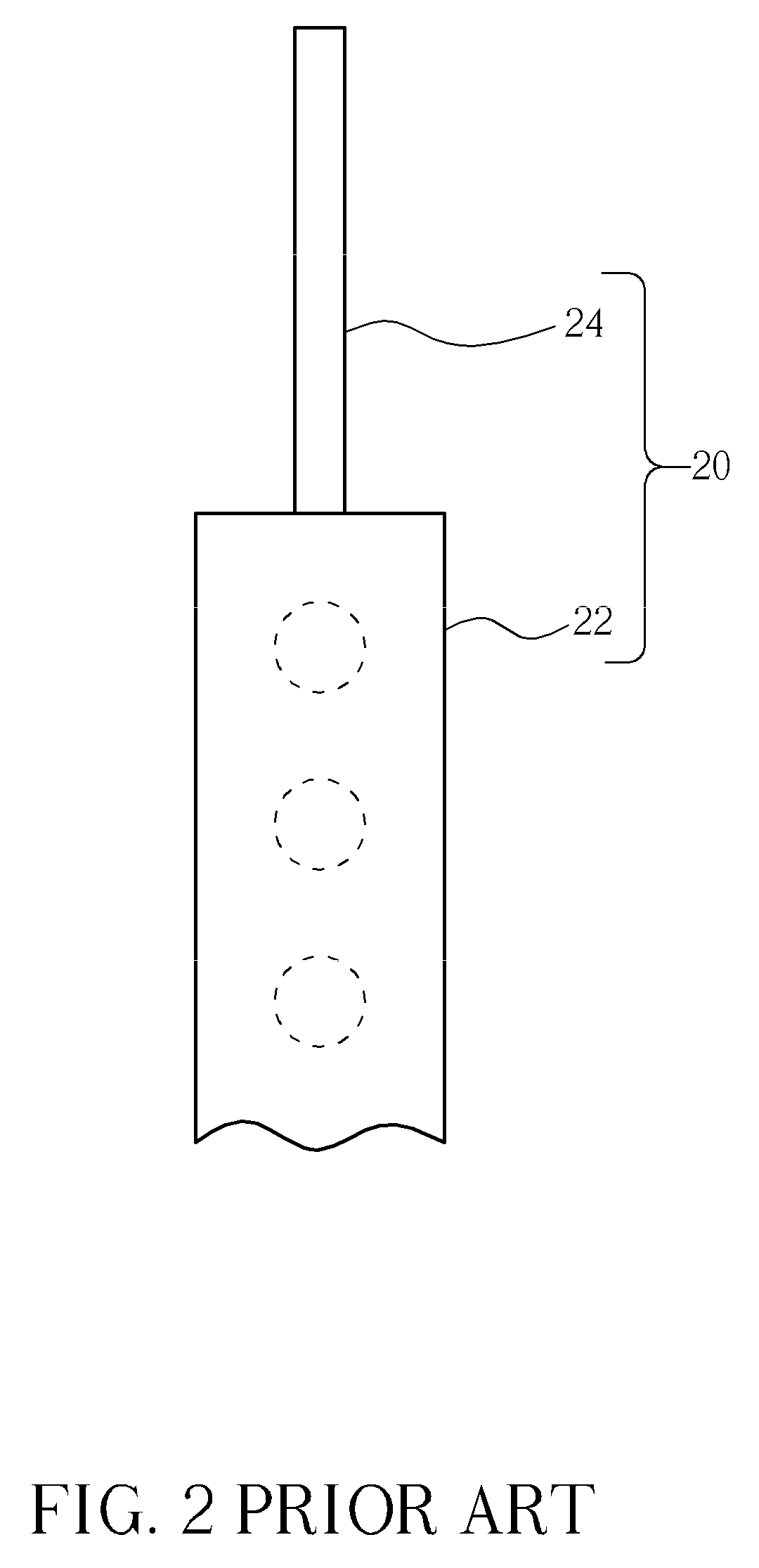
[0025]Please refer to FIG. 8. FIG. 8 is an amplified schematic diagram of the conductive wire pattern in a pad area 58 of the LCD panel of FIG. 7. The conductive wire pattern 60 includes a plurality of terminals 62 that are parallel to each other along the Y direction and arranged side by side along the X direction in FIG. 8. Each of the terminals 62 includes an opening portion 64 and a line portion 66. The opening portions ...


PUM


Abstract

A conductive line pattern of a pad area includes a plurality of terminals arranged side by side. Each terminal includes an opening portion that surrounds a bonding pad of the substrate and with a side edge and a line portion connecting with the side edge of the corresponding opening portion. The relative position of each line portion and the corresponding opening portion varies according to the location of the terminal in the pad area. A pattern of conductors (74) on a film (72) is to be bonded to the bonding pads at the openings (64) and the line portions (66) positional correspondence to the conductors (74) is used to detect alignment error. If any of the line (66) are located in the middle of a conductor (74) it serves to indicate an improper shift of the film (72).

Description

BACKGROUND OF THE INVENTION[0001]1. Field of the Invention[0002]The present invention is related to a conductive wire pattern of a pad area and a method of monitoring a bonding error of a film, and more particularly, to a conductive wire pattern of a pad area that can serve as a reference basis of monitoring a bonding error of a film and the method of monitoring the bonding error thereof.[0003]2. Description of the Prior Art[0004]An array substrate and a color filter (CF) substrate are separately fabricated in the general fabrication of a liquid crystal display (LCD). The fabrication of the array substrate includes several steps of semiconductor process such as thin film deposition, photolithography, and etching processes in order to fabricate thin film transistor (TFT) array. The CF substrate includes color filters corresponding to the TFTs or pixels in an array arrangement on a substrate. After the fabrication of the array substrate and the CF substrate are completed, attachment o...

Claims


Application Information

Patent Timeline
Patent Type & Authority Patents(United States)
IPC IPC(8): H05K1/00
CPCG02F1/1345G09G2300/0426
Inventor TENG, YIN-HSIANGHSU, HAN-TUNG
Owner CHUNGHWA PICTURE TUBES LTD
Why Eureka
Try Eureka