Touchpad with single-layered printed circuit board structure

a printed circuit board and touchpad technology, applied in the field of touchpads, can solve the problems of insufficient price to satisfy users' requirements, ineffective cost reduction of such touchpads, and shorter life of touchpads, and achieve the effect of low cos

Inactive Publication Date: 2012-04-03
ELAN MICROELECTRONICS CORPORATION
View PDF9 Cites 52 Cited by
  • Summary
  • Abstract
  • Description
  • Claims
  • Application Information

AI Technical Summary

Benefits of technology

[0006]An object of the present invention is to provide a low cost touchpad constructed with single-layered PCB structure.
[0007]Another object of the present invention is to provide a long lifetime touchpad constructed with single-layered PCB structure.

Problems solved by technology

Although the ground layer 112 is proven not necessary by experiments, thereby simplifying the four-layered PCB structure to three-layered structure, the cost of such touchpad is still not reduced effectively.
Although the touchpad with two-layered PCB structure has lower cost than that of the touchpad with four-layered PCB structure, it is still not enough to satisfy the requirement of users on the price.
Additionally, the carbon film wires printed on the two-layered PCB structure will be worn out as it is used, resulting in shorter lifetime of the touchpad.

Method used


Image

  • Touchpad with single-layered printed circuit board structure
  • Touchpad with single-layered printed circuit board structure
  • Touchpad with single-layered printed circuit board structure

Examples


Embodiment Construction

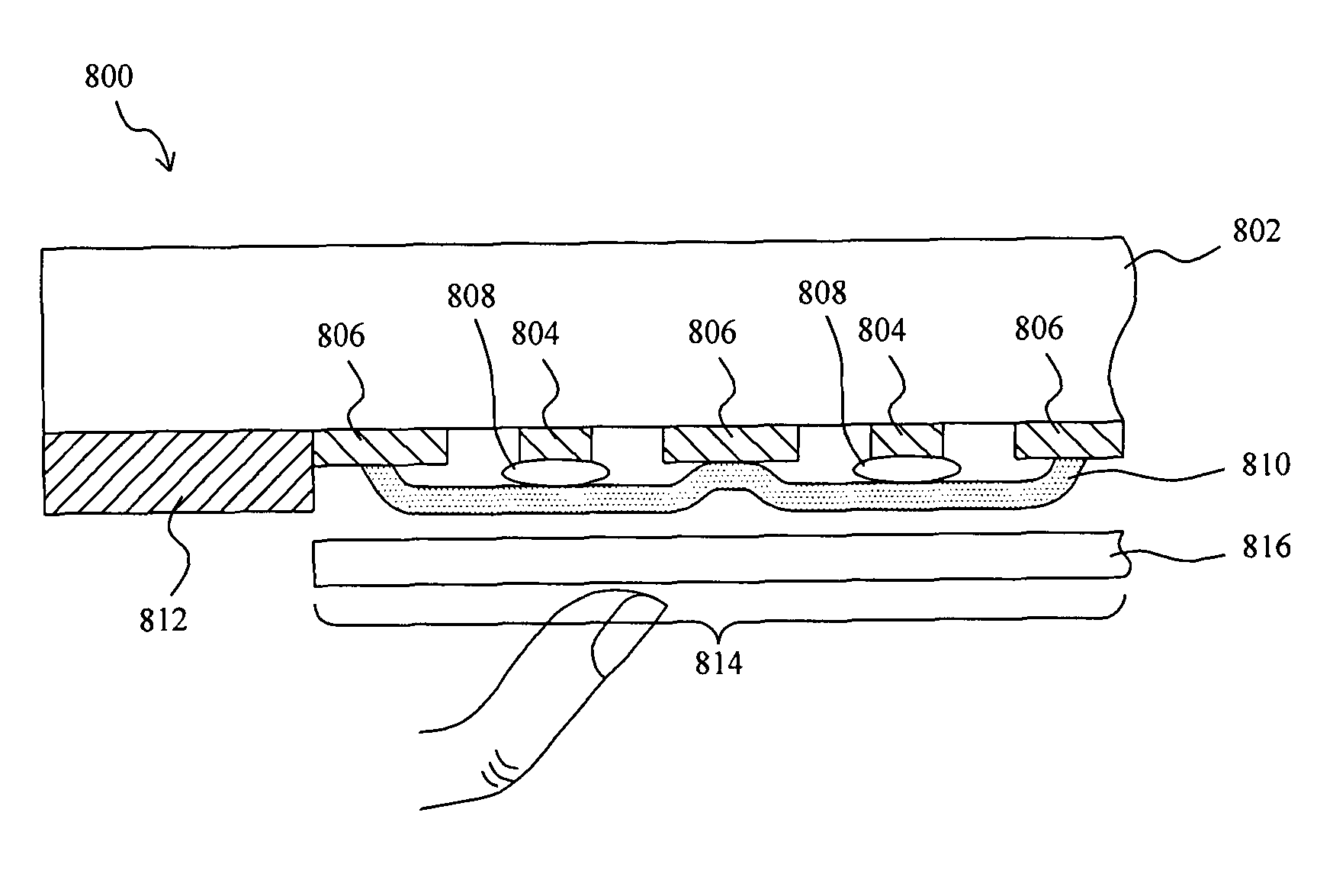
[0022]FIG. 8 shows a cross-sectional view 800 of a touchpad with single-layered PCB structure according to the present invention, in which a PCB 802 includes a bottom layer having two areas, i.e., sensor area 814 and component area 812 on the periphery of the sensor area 814, in the sensor area 814 there are X-directional traces 804 as shown in FIG. 3A and Y-directional traces 806 as shown in FIG. 3B, and an insulator cover 816 covers on the sensor area 814 for providing an operation area. In this embodiment, for the purpose of avoiding short circuit resulted from the intersections of the X-directional traces 804 and the Y-directional traces 806, the Y-directional traces 806 in the sensor area 814 are not interconnected therebetween, resulting in the signals not able to transmit along the Y-direction in the sensor area 814. Therefore, by using carbon ink printing, carbon film wires 810 are formed in the sensor area 814 to interconnect the Y-directional traces 806, and an insulator 8...


PUM


Abstract

In a touchpad with single-layered PCB structure, a PCB has a bottom layer with a sensor area and a component area thereon, the sensor area includes two directional traces directly connected to the component area, respectively, and carbon film wires in the sensor area for interconnecting one or more of the directional traces.

Description

FIELD OF THE INVENTION[0001]The present invention is generally related to a touchpad and, more particularly, to a touchpad with single-layered printed circuit board (PCB) structure.BACKGROUND OF THE INVENTION[0002]Touchpads have been widely used in electronic products including portable computers, personal digital assistants (PDAs), mobile phones, and other electronic systems. By sliding or touching on the operation area of a touchpad with a finger or other object, the relative movement or absolute coordinate movement of a cursor, or other extended functions such as simulated buttons, may be implemented. A conventional touchpad is constructed by a four-layered printed circuit board (PCB) structure, as shown by a cross-sectional view of FIG. 1, which comprises X-directional traces 104 provided in a first layer of a PCB 102, Y-directional traces 108 provided in a second layer of the PCB 102, an insulator layer 106 between the X-directional traces 104 and the Y-directional traces 108, ...

Claims


Application Information

Patent Timeline
Patent Type & Authority Patents(United States)
IPC IPC(8): G06F3/041
CPCG06F3/03547G06F3/0414
Inventor LII, JIA-YIHCHIU, YEN-CHANGCHIEN, YUNG-LIEH
Owner ELAN MICROELECTRONICS CORPORATION
Why Eureka
Try Eureka