Stack structure comprising epitaxial graphene, method of forming the stack structure, and electronic device comprising the stack structure

a stack structure and epitaxial graphene technology, applied in the field of stack structure comprising epitaxial graphene, can solve the problems of difficult to manufacture electronic devices including graphene structures, difficult to adjust the number, position and width of graphene layers, and difficult to obtain a large-surface graphene layer

Active Publication Date: 2012-04-17
SAMSUNG ELECTRONICS CO LTD
View PDF8 Cites 14 Cited by
  • Summary
  • Abstract
  • Description
  • Claims
  • Application Information

AI Technical Summary

Problems solved by technology

However, due to the difficulty of the process of manufacturing graphene, it is not easy to manufacture electronic devices including graphene structures.
However, when using this method, it is difficult to adjust the number, position, and width of graphene layers, since the method basically expects a coincidence, and it is also difficult to obtain a large-surface graphene layer.
Alternatively, a growth method of growing a graphene layer on a compound single crystal substrate has been suggested; however, the compound single crystal substrate is expensive, and it is difficult to manufacture a large-surface compound single crystal substrate.
In addition, the type of the compound single crystal substrate on which a graphene layer can be grown is very limited, and it is not easy to apply the compound single crystal substrate to most manufacturing processes of electronic devices.

Method used


Image

  • Stack structure comprising epitaxial graphene, method of forming the stack structure, and electronic device comprising the stack structure
  • Stack structure comprising epitaxial graphene, method of forming the stack structure, and electronic device comprising the stack structure
  • Stack structure comprising epitaxial graphene, method of forming the stack structure, and electronic device comprising the stack structure

Examples


Embodiment Construction

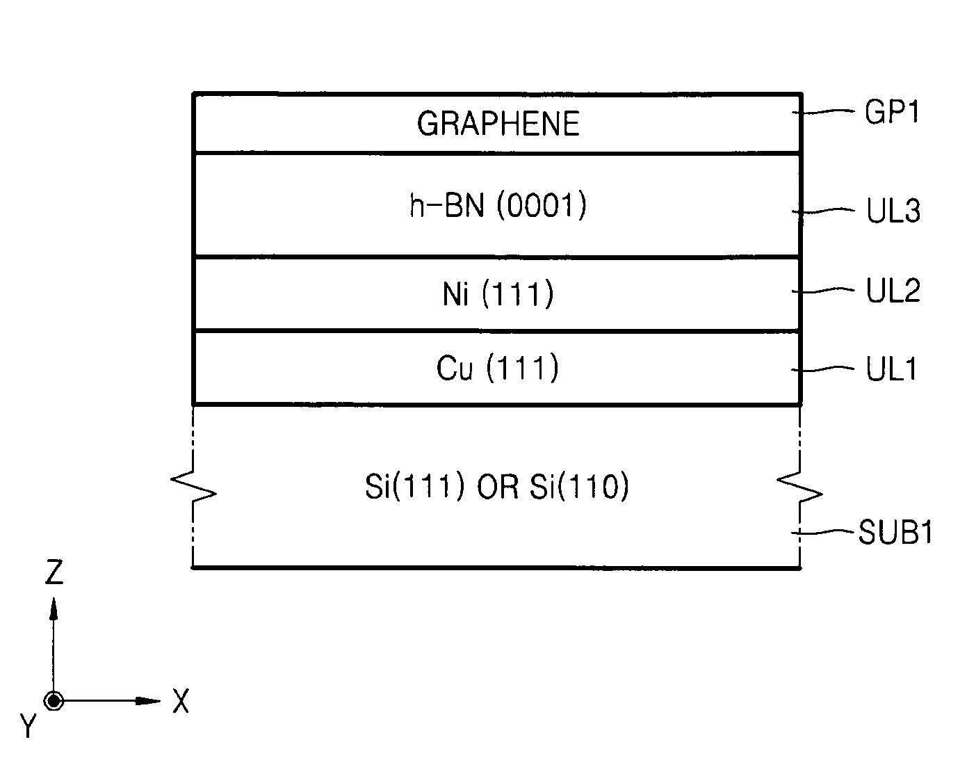
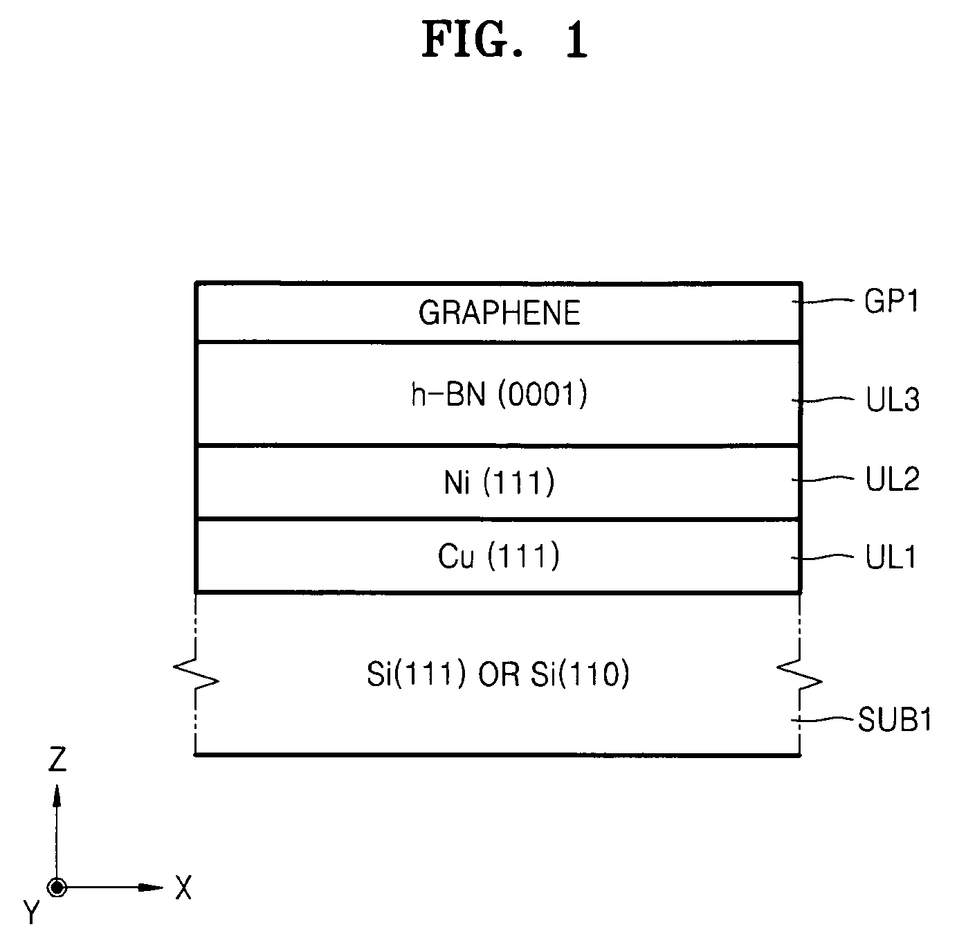
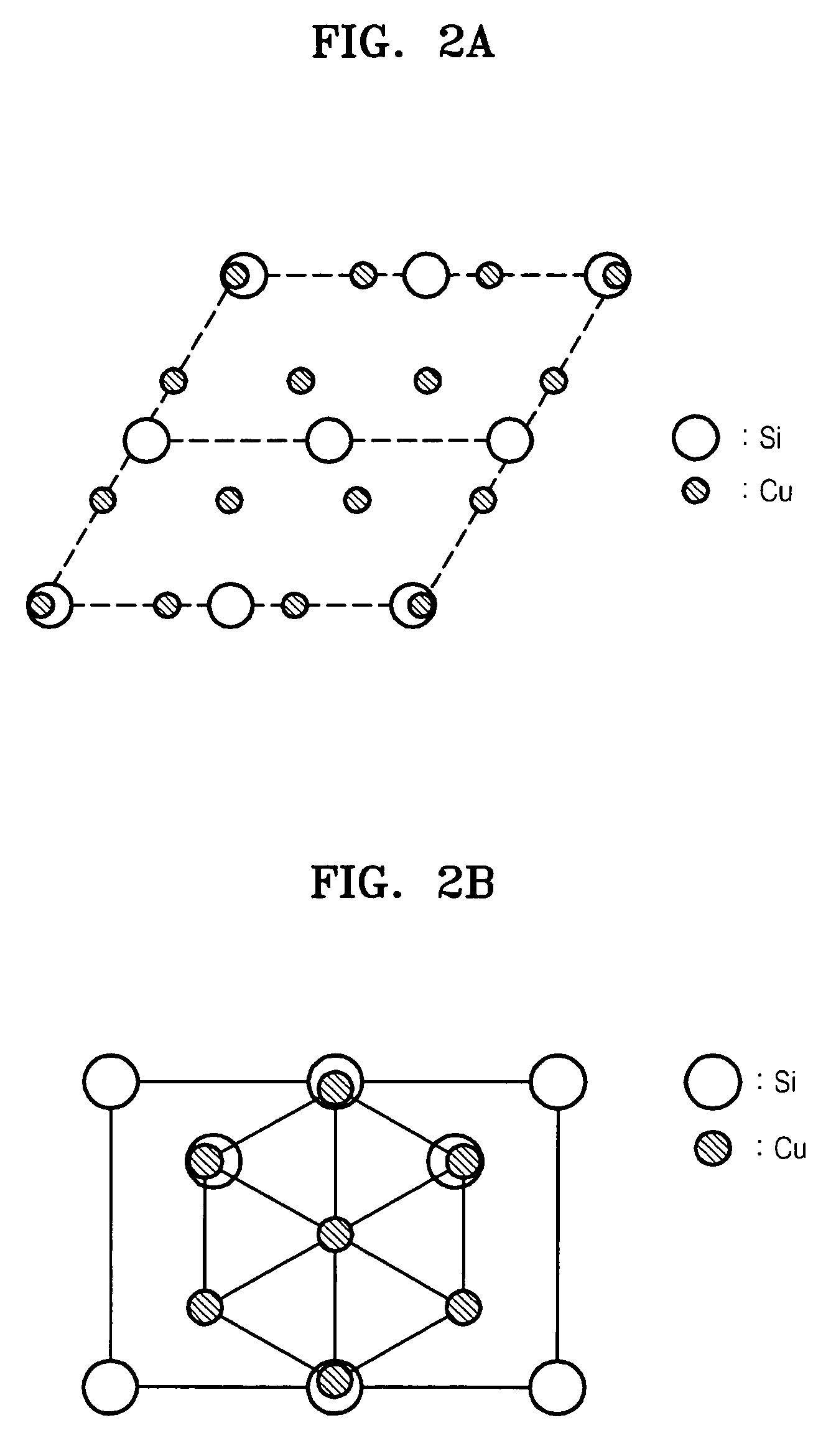
[0036]Various example embodiments will now be described more fully with reference to the accompanying drawings in which some example embodiments are shown. In the drawings, the thicknesses of layers and regions are exaggerated for clarity.

[0037]Detailed illustrative example embodiments are disclosed herein. However, specific structural and functional details disclosed herein are merely representative for purposes of describing example embodiments. This invention, however, may be embodied in many alternate forms and should not be construed as limited to only the example embodiments set forth herein.

[0038]Accordingly, while example embodiments are capable of various modifications and alternative forms, embodiments thereof are shown by way of example in the drawings and will herein be described in detail. It should be understood, however, that there is no intent to limit example embodiments to the particular forms disclosed, but on the contrary, example embodiments are to cover all mod...


PUM

PropertyMeasurementUnit
temperatureaaaaaaaaaa
stack structureaaaaaaaaaa

Abstract

Provided are a stack structure including an epitaxial graphene, a method of forming the stack structure, and an electronic device including the stack structure. The stack structure includes: a Si substrate; an under layer formed on the Si substrate; and at least one epitaxial graphene layer formed on the under layer.

Description

PRIORITY STATEMENT[0001]This application claims the benefit of Korean Patent Application No. 10-2008-0050467, filed on May 29, 2008 in the Korean Intellectual Property Office, the disclosure of which is incorporated herein in its entirety by reference.BACKGROUND[0002]1. Field[0003]The present invention relates to an electronic device, and more particularly, to a stack structure comprising an epitaxial graphene, a method of forming the stack structure, and an electronic device including the stack structure.[0004]2. Description of the Related Art[0005]Graphene is a hexagonal single-layer structure formed of carbon atoms. Graphene is chemically very stable, and has characteristics of a semi-metal in which a conduction band and a valence band are overlapped with only at one point, that is, at a Dirac point. Also, graphene shows 2-dimensional ballistic transport. A 2-dimensional ballistic transport of a charge in a medium, means that a charge is transported in a medium without resistance...

Claims


Application Information

Patent Timeline
Patent Type & Authority Patents(United States)
IPC IPC(8): H01L21/02
CPCB82Y10/00H01L21/02433H01L21/02447H01L21/02458H01L21/02491H01L21/02505H01L21/02516H01L21/02527H01L21/0262H01L29/045H01L29/0665H01L29/0673H01L29/16H01L29/1606H01L29/2003H01L29/267H01L29/7781H01L29/78684H01L21/02381Y10T428/12674
Inventor WOO, YUN-SUNGSEO, SUN-AEKIM, DONG-CHULCHUNG, HYUN-JONGJEON, DAE-YOUNG
Owner SAMSUNG ELECTRONICS CO LTD
Why Eureka
Try Eureka