
Efficient reduction of read disturb errors in NAND FLASH memory

a technology of nand flash memory and read disturb, which is applied in the direction of error detection/correction, fault response, instruments, etc., can solve the problems of unread cell read disturbance, no longer determined, and general efficiency of partial page operations

Inactive Publication Date: 2012-05-29
INT BUSINESS MASCH CORP
View PDF62 Cites 17 Cited by
  • Summary
  • Abstract
  • Description
  • Claims
  • Application Information

AI Technical Summary

Benefits of technology

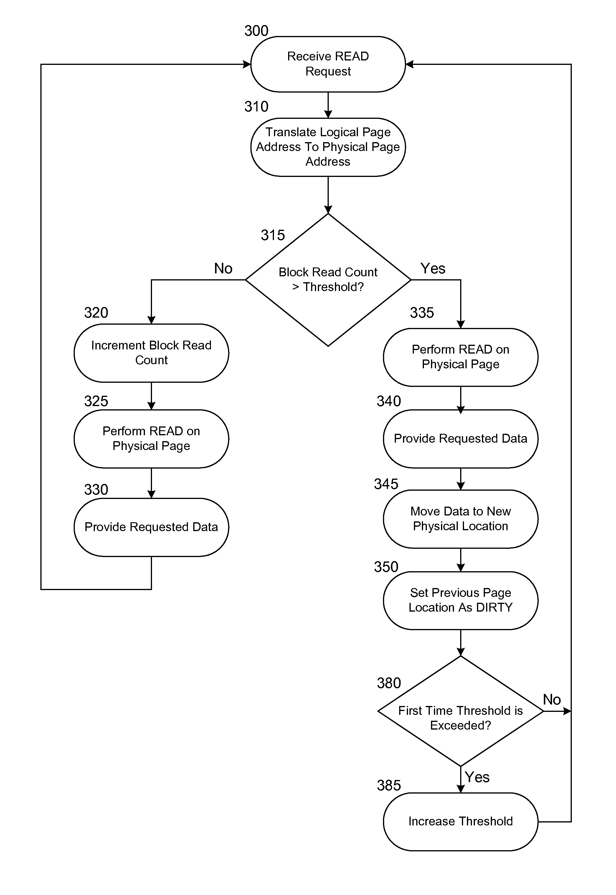
This approach significantly reduces Read Disturb errors by moving only affected data, thereby minimizing overhead and extending the device's useful life without the performance degradation caused by frequent block movements.

Problems solved by technology

While some flash memory devices support operations on “partial pages,” these partial page operations are generally less efficient than their complete page counterparts.
This weak programming resulting from the READ operation cannot always be predicted accurately and can result in a number of bits in memory cells not associated with the cells being read becoming corrupted such that one could no longer determine whether the originally stored data bit was a “1” or a “0.” Because the errors described above are induced by the disturbances created by the READ operation, they are known as “Read Disturb” errors.
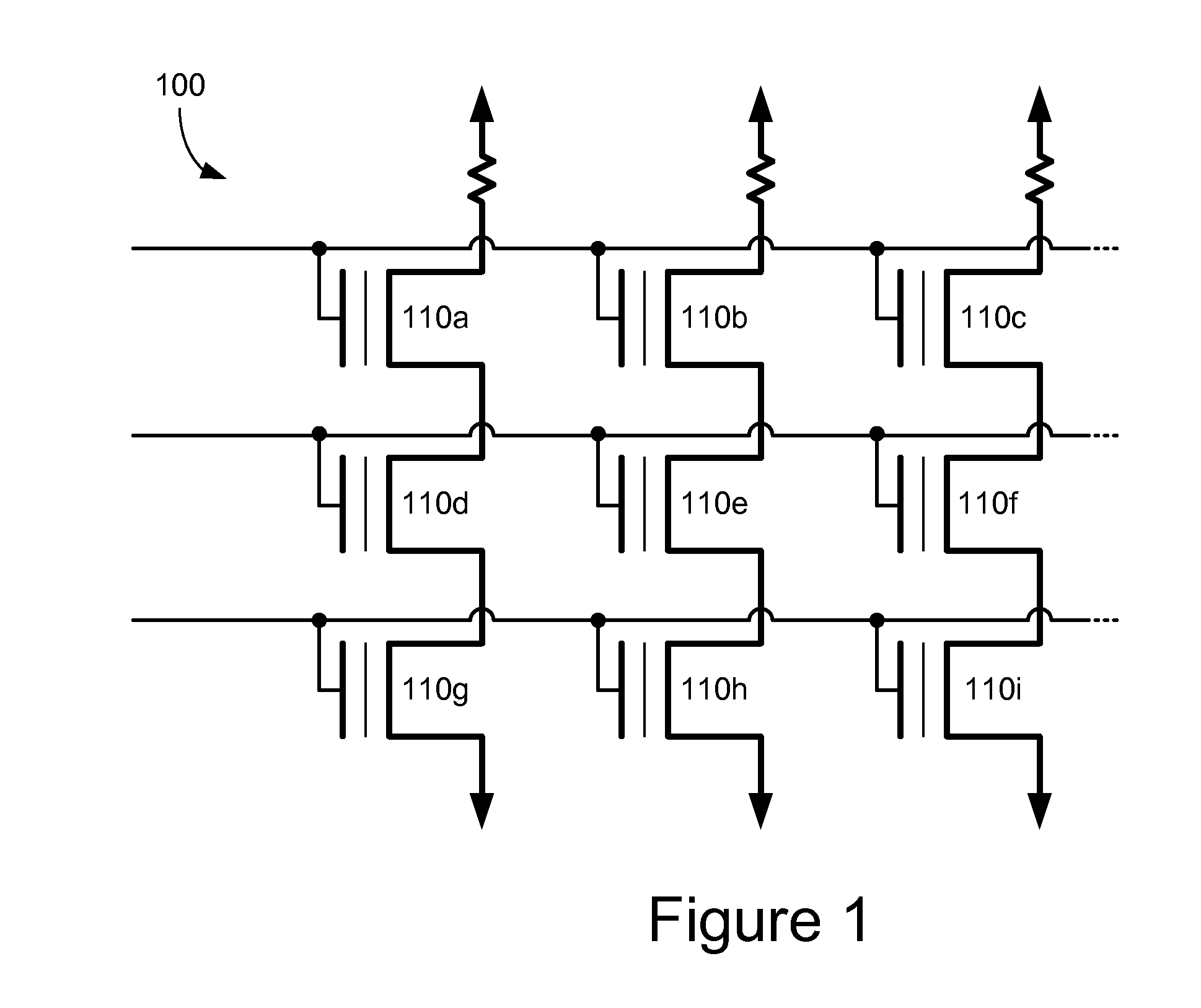
In such NAND FLASH memory devices, the control gates of unread cells are driven with a voltage that is guaranteed to render the unread cells conductive and that also leads to read disturbance in the unread cells.
MLC NAND FLASH memory is generally much more susceptible to read disturb errors than its SLC counterpart.
There are limitations associated with the use of ECC to address Read Disturb errors in NAND FLASH memory.
If more than one of the bits in the data item is disturbed, most ECC techniques will not be able to reconstruct the original data item.
Moreover, if a large number of bits in a data item are errantly disturbed, certain ECC techniques will be incapable of identifying the existence of an error.
Compounding this issue is the fact that Read Disturb errors occur in Pages that are not being read, while data and ECC bits must be read to perform checking and correction.
Hence, the number of errors in a disturbed page can grow from a correctable number to an uncorrectable number without any warning that the seriousness of the induced errors is increasing.
Thus, while ECC techniques may be widely utilized, they are not always effective.
While this approach can potentially avoid certain Read Disturb errors, it can limit the performance of a device or system utilizing this technique since the movement of the Block of data imposes burdens on the device or system in terms of overhead, speed, efficiency, power and other aspects that can degrade the overall performance of the device or system.
Not only does it take an appreciable amount of overhead in terms of processing power and time to move the entire Block of data, the ERASE operation for the original Block can be time consuming.
For systems where high speed read operations are desired, such burdens are undesirable and inefficient.
Another issue associated with the approach of maintaining a count and moving and erasing a data Block when the READ count for the Block is exceeded is that it imposes upon the system a relatively large number of ERASE operations.
In particular, because the entire contents of a Block are moved and erased each time the predetermined count for that Block is exceeded, the processing of the data in a given Block that includes multiple, frequently accessed Pages, will require a large number of ERASE operations over the lifetime of the product.
Because FLASH memory devices do not have unlimited lifetimes and because a given FLASH memory cell is subject to failure upon the occurrence of a given number of ERASE operations that will vary from manufacturer to manufacturer and from device to device, the described system tends to shorten the overall useful life of the devices within a FLASH memory system.

Method used


Image

  • Efficient reduction of read disturb errors in NAND FLASH memory
  • Efficient reduction of read disturb errors in NAND FLASH memory
  • Efficient reduction of read disturb errors in NAND FLASH memory

Examples


Embodiment Construction

[0043]The Figures described above and the written description of specific structures and functions below are not presented to limit the scope of what Applicants have invented or the scope of the appended claims. Rather, the Figures and written description are provided to teach any person skilled in the art to make and use the inventions for which patent protection is sought. Those skilled in the art will appreciate that not all features of a commercial embodiment of the inventions are described or shown for the sake of clarity and understanding. Persons of skill in this art will also appreciate that the development of an actual commercial embodiment incorporating aspects of the present inventions will require numerous implementation-specific decisions to achieve the developer's ultimate goal for the commercial embodiment. Such implementation-specific decisions may include, and likely are not limited to, compliance with system-related, business-related, government-related and other c...


PUM


Abstract

Methods and apparatuses for reduction of Read Disturb errors in a NAND FLASH memory system comprise a controller configured to organize FLASH memory devices into blocks, each block having a plurality of pages, and each page defining an individually addressable physical memory location. The controller is further configured to accumulate a Block READ Count corresponding to the number of times any pages in a first block of pages have been read since the first block was last erased. Once the READ count reaches a predetermined number, the controller responds to subsequent READ requests for pages within the first block by moving data associated with a requested page to a page in a second, different block without moving data associated with other pages in the first block, and modifying a logical-to-physical translation table to associate the moved data with the physical address of the page in the second block.

Description

CROSS REFERENCE TO RELATED APPLICATIONS[0001]This application is a continuation of U.S. Non-Provisional application Ser. No. 12 / 566,421, which issued as U.S. Pat. No. 7,818,525, entitled “Efficient Reduction of Read Disturb Errors in NAND FLASH Memory,” filed Sep. 24, 2009, and which claims priority to U.S. Provisional Application Ser. No. 61 / 233,218, entitled “Efficient Reduction of Read Disturb Errors in NAND FLASH Memory,” filed Aug. 12, 2009, both of which are incorporated herein by reference.STATEMENT REGARDING FEDERALLY SPONSORED RESEARCH[0002]Not applicable.REFERENCE TO APPENDIX[0003]Not applicable.BACKGROUND OF THE INVENTION[0004]1. Field of the Invention:[0005]This disclosure relates generally to methods and apparatus for reducing or eliminating certain data errors associated with FLASH memory devices utilizing a NAND architecture.[0006]2. Description of the Related Art:[0007]In general, a FLASH memory device is one type of memory device that can retain stored digital data,...

Claims


Application Information

Patent Timeline
Patent Type & Authority Patents(United States)
IPC IPC(8): G06F12/00
CPCG06F12/0246G06F2212/7205G06F2212/1032G06F11/076G06F11/1072G11C29/50004G11C2029/5004G06F3/0619G06F3/0647G06F3/0679G06F12/1009G06F2212/7201
Inventor FROST, HOLLOWAY H.CAMP, CHARLES J.FISHER, TIMOTHY J.FUXA, JAMES A.SHELTON, LANCE W.
Owner INT BUSINESS MASCH CORP
Learn More