Flash memory fabrication method

a technology of flash memory and fabrication method, which is applied in the direction of semiconductor devices, instruments, electrical equipment, etc., can solve the problems of affecting the efficiency of programming and erasing, and unable to store enough charge, etc., to achieve the effect of efficient reduction of read disturb errors

Active Publication Date: 2018-11-06
SEMICON MFG INT (SHANGHAI) CORP
View PDF9 Cites 1 Cited by
  • Summary
  • Abstract
  • Description
  • Claims
  • Application Information

AI Technical Summary

Benefits of technology

[0007]Embodiments of the present invention provide a semiconductor device including a Flash memory device, and a method for manufacturing such semiconductor device that can ensure efficient reduction of read disturb errors of the Flash memory device.

Problems solved by technology

In Flash memory devices such as p-Flash, under repeated programming and erasing operations, the high voltage programming can damage the tunnel oxide layer, so that enough stored charge can be lost through the damaged tunnel oxide, leading to erase / read disturb errors.
However, this approach of increasing the thickness of portion 1011 of tunnel oxide layer 101 at the edge of the active region also increases the thickness of the portion of tunnel oxide layer 101 located in the center region of the active region, and this will adversely affect the programming and erasing efficiency.
As is described above, it is difficult to ensure the programming and erasing performance while reducing read and erase disturbance.

Method used


Image

  • Flash memory fabrication method
  • Flash memory fabrication method
  • Flash memory fabrication method

Examples


embodiment 1

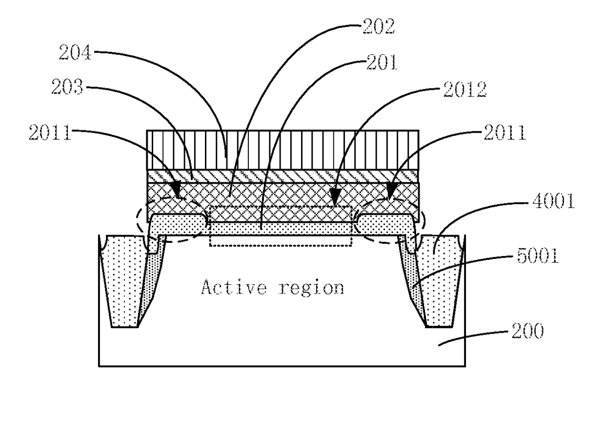
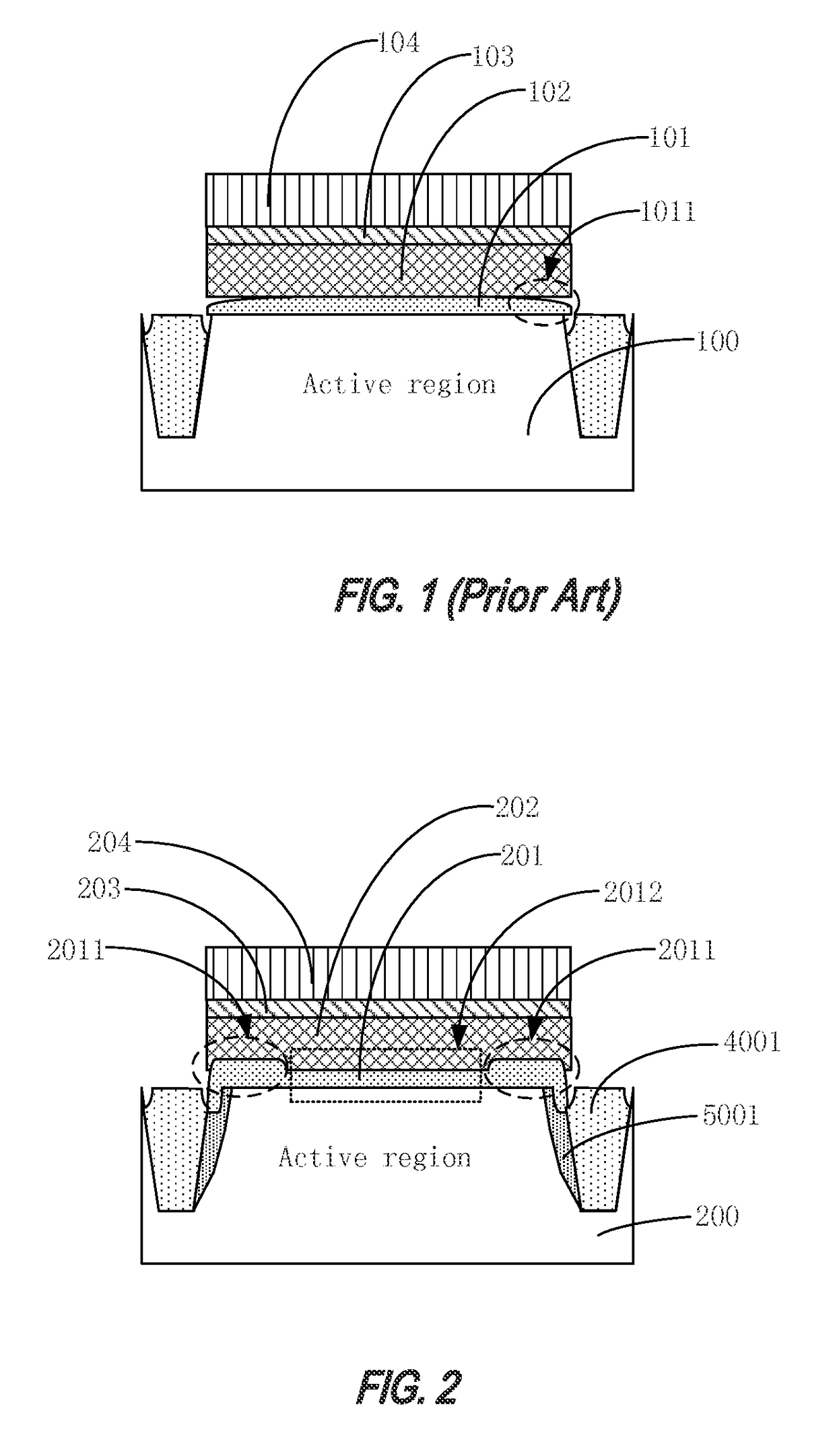
[0033]Embodiments of the present invention provide a semiconductor device such as a Flash memory device (e.g., p-Flash), or a semiconductor device containing a flash memory device. FIG. 2 is a simplified cross-sectional view of a semiconductor device according to an embodiment of the present invention.

[0034]Referring to FIG. 2, a semiconductor device includes a semiconductor substrate 200, a tunnel oxide layer 201 disposed on semiconductor substrate 200, a floating gate 202 on tunnel oxide layer 201, an interlayer dielectric layer 203 on floating gate 202, and a control gate 204 on interlayer dielectric layer 203. In the embodiment, the thickness of a portion 2011 of tunnel oxide layer 201 disposed on an edge of the active region is greater than the thickness of a portion 2012 of tunnel oxide layer 201 disposed in the center of the active region. The term “edge of an active region” will be used herein to refer to edges or peripheral region away from the center of the active region. ...

embodiment 2

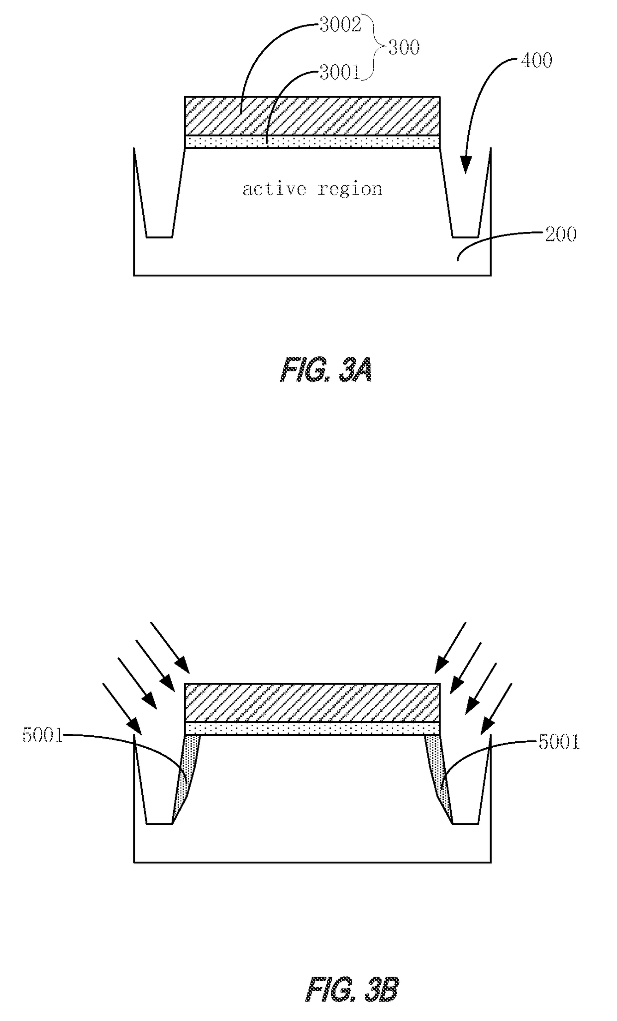
[0040]FIGS. 3A through 3H are simplified cross-sectional views of intermediate structures at different stages of a semiconductor device according to an embodiment of the present invention. FIG. 4 is a flow chart of a method for manufacturing a semiconductor device according to an embodiment of the present invention.

[0041]With reference to FIGS. 3A-3H and FIG. 4, a method for manufacturing a semiconductor device according to an embodiment of the present invention will be described in detail. The method may include the following steps:

[0042]Step A1: provide a semiconductor substrate 200 including an active region; form a hard mask 300 on the semiconductor substrate; etch the semiconductor substrate using the hard mask layer as a mask to form a trench 400 in the semiconductor substrate on opposite sides of the active region, as shown in FIG. 3A.

[0043]In an embodiment, hard mask 300 may include a first hard mask layer 3001 and a second hard mask layer 3002 overlying the first hard mask ...

embodiment 3

[0077]Embodiments of the present invention provide an electronic device, which may include an electronic component and a semiconductor device electrically connected to the electronic component. The semiconductor device can be manufactured according to the above-described method.

[0078]In an embodiment, the semiconductor device may include a semiconductor substrate, a tunnel oxide layer on the semiconductor substrate, a floating gate on the tunnel oxide layer, a gate dielectric layer on the floating gate, and a control gate on the gate dielectric layer. The portion of the tunnel oxide layer disposed on the edge of the active region has a thickness greater than the thickness of the portion of the tunnel oxide layer disposed on the center (i.e., away from the edge) of the active region.

[0079]In an embodiment, the electronic device may include a semiconductor device fabricated using the above-described method. The electronic device may be a mobile phone, a laptop, a netbook, a tablet PC,...


PUM


Abstract

A semiconductor device and a method of fabricating the same are provided. The semiconductor device includes a semiconductor substrate comprising an active region, and successive layers of a tunnel oxide layer, a floating gate, a gate dielectric layer, a control gate overlying each other. A first portion of the tunnel oxide layer disposed on an edge of the active region has a thickness that is greater than a thickness of a second portion of the tunnel oxide layer disposed away from the edge of the active region. Such features ensure efficient reduction of read disturb errors of a Flash memory device.

Description

CROSS-REFERENCES TO RELATED APPLICATIONS[0001]This application claims priority to Chinese patent application No. 201410432340.1, filed on Aug. 28, 2014, the content of which is incorporated herein by reference in its entirety.BACKGROUND OF THE INVENTION[0002]The present invention relates to semiconductor devices, and more particularly to a semiconductor device and method for manufacturing the same.[0003]Flash memory devices are widely used in various products due to their advantages such as data-holding capability. In Flash memory devices such as p-Flash, under repeated programming and erasing operations, the high voltage programming can damage the tunnel oxide layer, so that enough stored charge can be lost through the damaged tunnel oxide, leading to erase / read disturb errors.[0004]FIG. 1 is a simplified cross-sectional view of a conventional structure of a semiconductor device containing a flash memory. The conventional structure includes a semiconductor substrate 100, a tunnel o...

Claims


Application Information

Patent Timeline
Patent Type & Authority Patents(United States)
IPC IPC(8): H01L21/28H01L29/423H01L29/66H01L29/10H01L29/06G11C16/34
CPCH01L21/28273H01L29/42324H01L29/66825H01L29/1083G11C16/3427H01L29/0649H01L29/40114H10B41/30
Inventor LIU, JINHUA
Owner SEMICON MFG INT (SHANGHAI) CORP
Why Eureka
Try Eureka