Method for manufacturing a resistive switching memory device and devices obtained thereof

a resistive switching and memory device technology, applied in semiconductor devices, digital storage, instruments, etc., can solve the problems of severe scaling problems of flash memory technology, and achieve the effect of facilitating the integration of resistive switching materials and higher integration densities

Active Publication Date: 2012-06-26
INTERUNIVERSITAIR MICRO ELECTRONICS CENT (IMEC VZW)
View PDF11 Cites 26 Cited by
  • Summary
  • Abstract
  • Description
  • Claims
  • Application Information

AI Technical Summary

Benefits of technology

[0025]Alternatively, modifying the conductive properties of at least part of the sidewall conductive layer may also occur during the step of providing a resistive layer, for example during oxidizing the metal thereby forming a metal-oxide material. This may for example be done for a sidewall conductive layer with a thickness Ts which is larger than 10 nanometers. Such a thickness may be achieved by using ALD or CVD for forming the conductive layer. This has the advantage that no separate step needs to be carried out for modifying the conductive properties of at least part of the sidewall conductive layer.
[0035]It is an advantage of embodiments of the present invention that a resistor element comprising a resistive switching layer may be manufactured which is scalable for at least several technology generations from the 45 nm CMOS node and beyond.
[0036]It is another advantage of embodiments of the present invention that the resistive memory element is directly stacked on top of the transistor. The resistive memory element is thus preferably formed at the M0 wiring local interconnect level, i.e. using the first contact to the transistor. Thereby higher integration densities are possible compared to the higher metal interconnect levels.
[0037]It is another advantage of embodiments of the present invention that a resistive memory device may be manufactured using technology and materials which are compatible with present and future generations of CMOS. The method according to embodiments of the present invention facilitates the integration of resistive switching materials in CMOS compatible process flows, more specifically in the CMOS compatible back-end-of-line (BEOL) processes.
[0038]It is another advantage of embodiments of the present invention that nonvolatile memory devices may be manufactured which allow integration into different memory architectures that can lead to different memory products and applications.

Problems solved by technology

However it is expected that Flash memory technology will face severe scaling problems beyond the 45 nm technology node due to fundamental physical and / or cost limitations.

Method used


Image

  • Method for manufacturing a resistive switching memory device and devices obtained thereof
  • Method for manufacturing a resistive switching memory device and devices obtained thereof
  • Method for manufacturing a resistive switching memory device and devices obtained thereof

Examples


Embodiment Construction

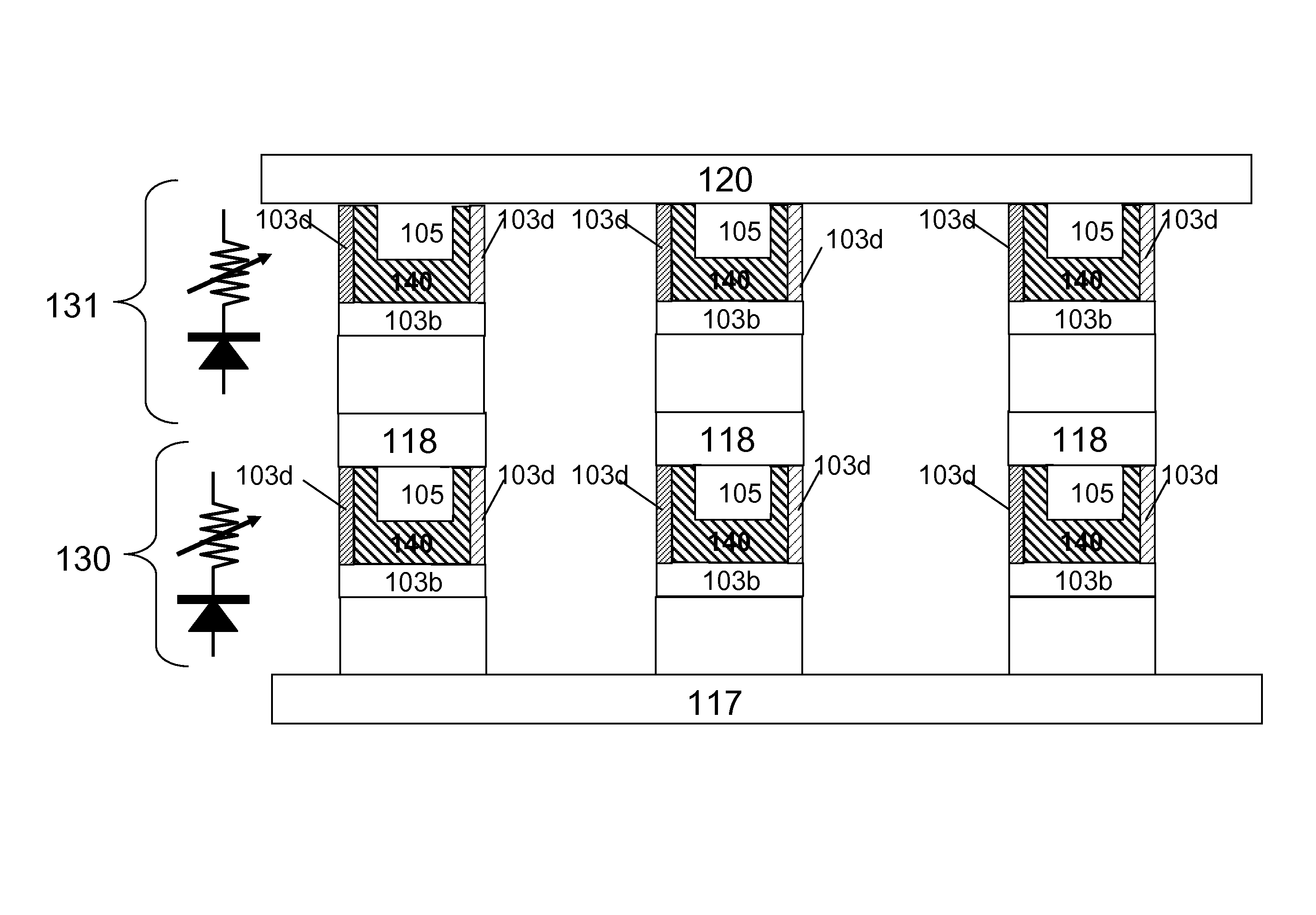
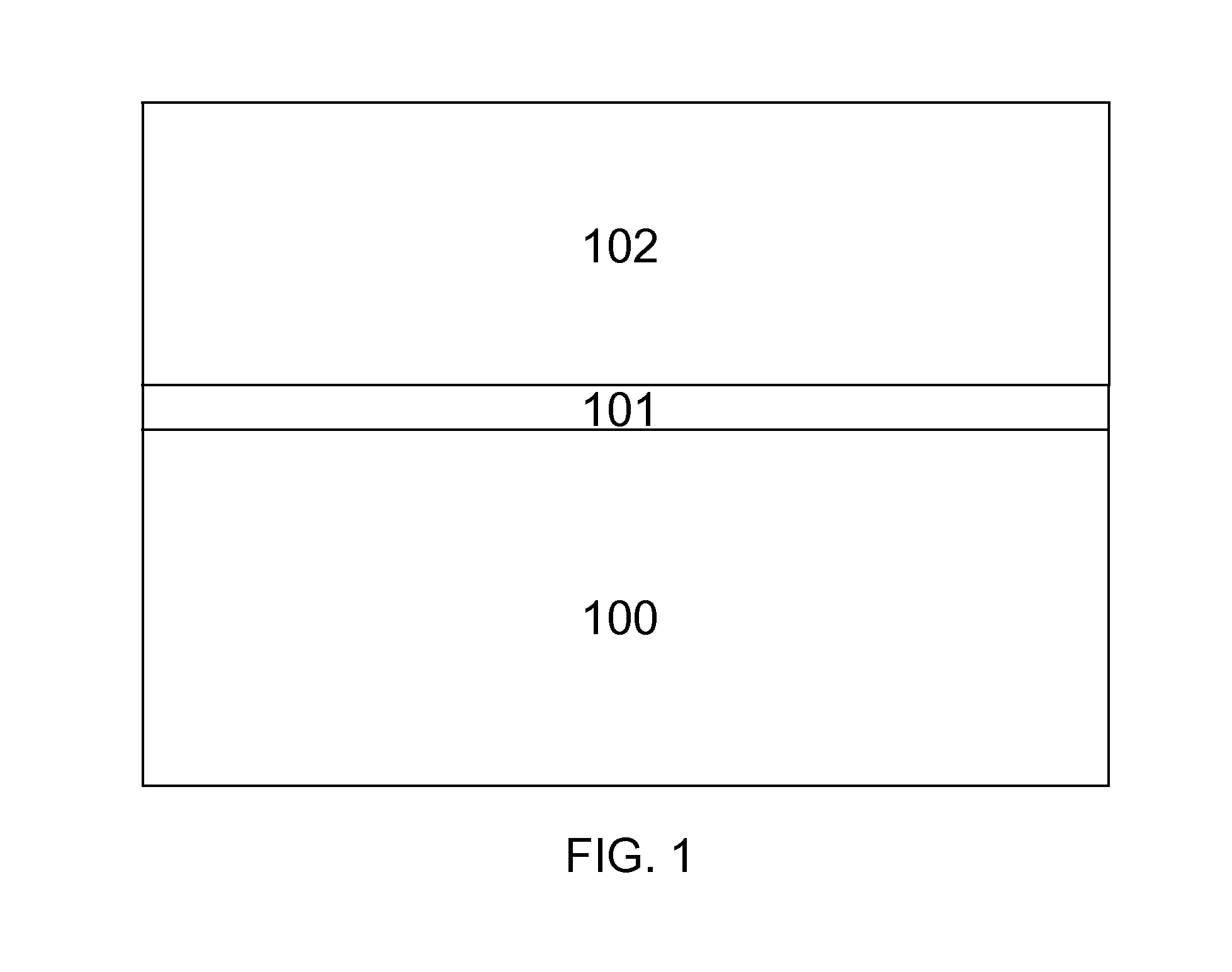
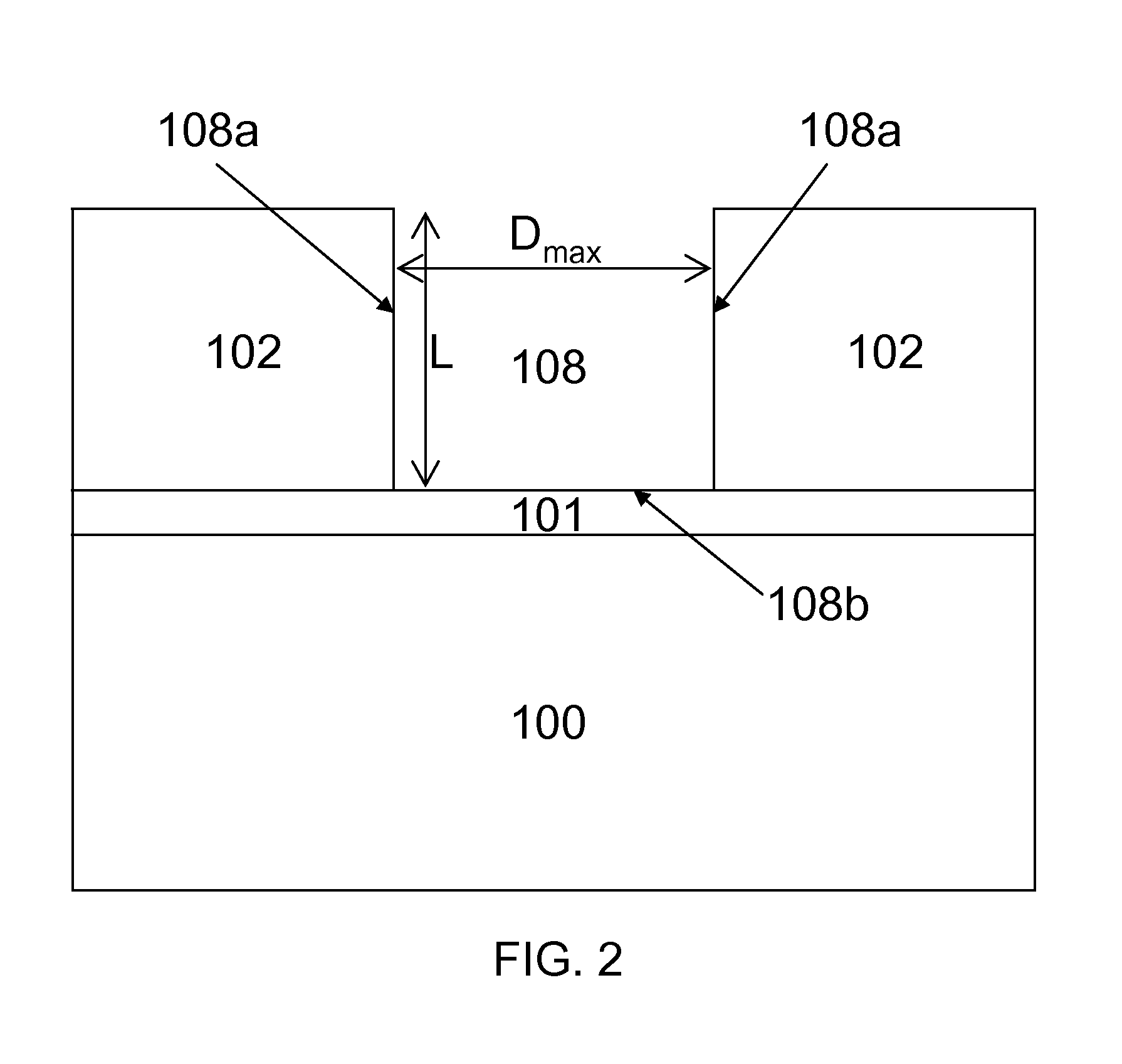
[0048]One or more embodiments of the present invention will now be described in detail with reference to the attached figures; the invention is, however, not limited thereto. The drawings described are only schematic and are non-limiting. In the drawings, the size of some of the elements may be exaggerated and not drawn on scale for illustrative purposes. The dimensions and the relative dimensions do not necessarily correspond to actual reductions to practice. Those skilled in the art can recognize numerous variations and modifications that are encompassed by the scope of the invention. Accordingly, the description of preferred embodiments should not be deemed to limit the scope of the present claims.

[0049]Furthermore, the terms first, second and the like in the description are used for distinguishing between similar elements and not necessarily for describing a sequential or chronological order. It is to be understood that the terms so used are interchangeable under appropriate cir...


PUM


Abstract

A method for manufacturing a resistive switching memory device comprises providing a substrate comprising an electrical contact, providing on the substrate a dielectric layer comprising a trench exposing the electrical contact, and providing in the trench at least the bottom electrode and the resistive switching element of the resistive memory device. The method may furthermore comprise providing a top electrode at least on or in the trench, in contact with the resistive switching element. The present invention also provides corresponding resistive switching memory devices.

Description

CROSS REFERENCE TO RELATED APPLICATIONS[0001]This application claims priority to U.S. Provisional Patent Application Ser. No. 61 / 140,762 filed on Dec. 24, 2008, and European Patent Application No. 09153091.5 filed on Feb. 18, 2009, the contents of which are incorporated by reference herein in its entirety.FIELD OF THE INVENTION[0002]The present invention generally relates to methods for manufacturing nonvolatile memory devices. More specifically it relates to methods for manufacturing resistive memory devices and to nonvolatile resistive memory devices thus manufactured.BACKGROUND OF THE INVENTION[0003]The evolution of the market of data storage memories indicates a growing need for ever-larger capacity, ranging from gigabytes to hundreds of gigabytes or even to terabytes. This evolution is driven, amongst others, by new data consuming applications such as multimedia and gaming. Flash memory technology, for example, which uses the shift in threshold voltage of a field effect transis...

Claims


Application Information

Patent Timeline
Patent Type & Authority Patents(United States)
IPC IPC(8): H01L21/00H01L21/20
CPCH01L45/04H01L45/1233H01L45/146H01L45/1608H01L27/2409H01L27/2436H01L27/2481H10B63/20H10B63/30H10B63/84H10N70/20H10N70/021H10N70/826H10N70/8833
Inventor REYES, JUDIT GLORIA LISONIGOUX, LUDOVICWOUTERS, DIRK
Owner INTERUNIVERSITAIR MICRO ELECTRONICS CENT (IMEC VZW)
Why Eureka
Try Eureka