

Semiconductor device and method for production of semiconductor device
a semiconductor and semiconductor technology, applied in the direction of semiconductor devices, electrical devices, transistors, etc., can solve the problems of weakened, stress applied to the channel part of the semiconductor layer, stress applied to the channel part stress applied to the channel part from the semiconductor layer, etc., to achieve the effect of improving the performance of the semiconductor device and improving the mobility of the carrier
- Summary
- Abstract
- Description
- Claims
- Application Information
AI Technical Summary
Benefits of technology
Problems solved by technology
Method used
Image

Examples
first embodiment
Structure of the Semiconductor Device
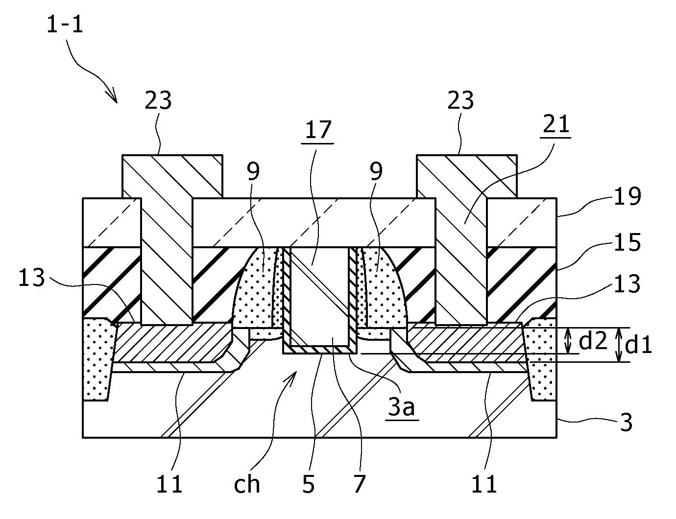
[0033]FIG. 1 is a sectional view showing important parts of the semiconductor device 1-1 according to the first embodiment of the present invention. The semiconductor device 1-1 shown in this figure is a semiconductor device of field-effect transistor type. It is constructed in the following manner.
[0034]The semiconductor device is formed on the semiconductor substrate 3 of single crystal silicon. The semiconductor substrate 3 has the recess 3a which is formed by digging the surface thereof. On the semiconductor substrate 3 is formed the gate electrode 7 which fills the recess 3a, with the gate insulating film 5 interposed therebetween. On both sides of the gate electrode 7 are formed the insulating side walls 9. On that surface of the semiconductor substrate 3, which is adjacent to both sides of the gate electrode 7 having the side walls 9, is formed the source-drain diffusion layer 11. The source-drain diffusion layer 11 has its surface covered...
second embodiment
Structure of the Semiconductor Device
[0076]FIG. 3 is a sectional view showing important parts of the semiconductor device 1-2 according to the second embodiment of the present invention. The semiconductor device 1-2 shown in this figure is a semiconductor device of field-effect transistor type. It differs from that according to the first embodiment explained above with reference to FIG. 1 in that that part of the surface of the semiconductor substrate 3 on which there are formed the source-drain diffusion layer 11 and the silicide film (stress applying layer) 13 is dug by recess etching. Except for this, its structure is identical with the structure according to the first embodiment.
[0077]As in the first embodiment, the semiconductor device is formed on the semiconductor substrate 3 of single crystal silicon. The semiconductor substrate 3 has the recess 3a which is formed by digging the surface thereof. On the semiconductor substrate 3 is formed the gate electrode 7 which fills the ...
third embodiment
Structure of the Semiconductor Device
[0101]FIG. 5 is a sectional view showing important parts of the semiconductor device 1-3 according to the third embodiment of the present invention. The semiconductor device 1-3 shown in this figure is a semiconductor device of field-effect transistor type. It differs from that according to the first embodiment explained above with reference to FIG. 1 in that the gate insulating film 5 does not entirely covers the inner wall of the groove pattern 17 but permits the upper part of the inner wall to expose itself. Except for this, its structure is identical with the structure according to the first embodiment.
[0102]As in the first embodiment, the semiconductor device is formed on the semiconductor substrate 3 of single crystal silicon. The semiconductor substrate 3 has the recess 3a which is formed by digging the surface thereof. On the semiconductor substrate 3 is formed the gate electrode 7 which fills the recess 3a, with the gate insulating film ...
PUM
 Abstract
Description
Claims
Application Information